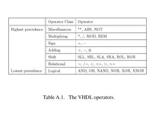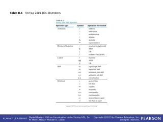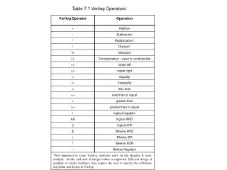
Table 7.1 Verilog Operators.
180 likes | 318 Views
Table 7.1 Verilog Operators. module gatenetwork ( A, B, C, D, X, Y ); input A ; input B ; input C ; input [2:1] D ; output X, Y ; reg Y ; // concurrent assignment statement wire X = A & ~( B | C ) & ( D [1] ^ D [2]);

Table 7.1 Verilog Operators.
E N D
Presentation Transcript
module gatenetwork(A, B, C, D, X, Y); input A; input B; input C; input [2:1] D; output X, Y; reg Y; // concurrent assignment statement wire X = A & ~(B|C) & (D[1] ^ D[2]); /* Always concurrent statement- sequential execution inside */ always @( A or B or C or D) Y = A & ~(B|C) & (D[1] ^ D[2]); endmodule
module DEC_7SEG(Hex_digit, segment_a, segment_b, segment_c, segment_d, segment_e, segment_f, segment_g); input [3:0] Hex_digit; output segment_a, segment_b, segment_c, segment_d; output segment_e, segment_f, segment_g; reg [6:0] segment_data; always @(Hex_digit) /* Case statement implements a logic truth table using gates*/ case (Hex_digit) 4’b 0000: segment_data = 7'b 1111110; 4’b 0001: segment_data = 7'b 0110000; 4’b 0010: segment_data = 7'b 1101101; 4’b 0011: segment_data = 7'b 1111001; 4’b 0100: segment_data = 7'b 0110011; 4’b 0101: segment_data = 7'b 1011011; 4’b 0110: segment_data = 7'b 1011111; 4’b 0111: segment_data = 7'b 1110000; 4’b 1000: segment_data = 7'b 1111111; 4’b 1001: segment_data = 7'b 1111011; 4’b 1010: segment_data = 7'b 1110111; 4’b 1011: segment_data = 7'b 0011111; 4’b 1100: segment_data = 7'b 1001110; 4’b 1101: segment_data = 7'b 0111101; 4’b 1110: segment_data = 7'b 1001111; 4’b 1111: segment_data = 7'b 1000111; default: segment_data = 7'b 0111110; endcase
/* Multiplexer example shows three ways to model a 2 to 1 mux */ module multiplexer(A, B, mux_control, mux_out1, mux_out2, mux_out3); input A; /* Input Signals and Mux Control */ input B; input mux_control; output mux_out1,mux_out2, mux_out3; reg mux_out2, mux_out3; /* Conditional Continuous Assignment Statement *//* works like an IF - ELSE */ wire mux_out1 = (mux_control)? B:A; /* If statement inside always statement */ always @(A or B or mux_control) if (mux_control) mux_out2 = B; else mux_out2 = A; /* Case statement inside always statement */ always @(A or B or mux_control) case (mux_control) 0: mux_out3 = A; 1: mux_out3 = B; default: mux_out3 = A; endcase endmodule
module tristate (a, control, tri_out); input a, control; output tri_out; reg tri_out; always @(control or a) if (control) /* Assignment of Z value generates a tri-state output */ tri_out =1'bZ; else tri_out = a; endmodule
module DFFs(D, clock, reset, enable, Q1, Q2, Q3, Q4); input D; input clock; input reset; input enable; output Q1, Q2, Q3, Q4; reg Q1, Q2, Q3, Q4; /* Positive edge triggered D flip-flop */ always @(posedge clock) Q1 = D; /* Positive edge triggered D flip-flop */ /* with synchronous reset */ always @(posedge clock) if (reset) Q2 = 0; else Q2 = D; /* Positive edge triggered D flip-flop */ /* with asynchronous reset */ always @(posedge clock or posedge reset) if (reset) Q3 = 0; else Q3 = D; /* Positive edge triggered D flip-flop */ /* with asynchronous reset and enable */ always @(posedge clock or posedge reset) if (reset) Q4 = 0; else if (enable) Q4 = D; endmodule
module ilatch( A, B, Output1, Output2); input A, B; output Output1, Output2; reg Output1, Output2; always@( A or B) if (!A) begin Output1 = 0; Output2 = 0; end else if (B) begin Output1 = 1; Output2 = 1; end else /*latch inferred since no value */ Output1 = 0; /*is assigned to Output2 here */ endmodule
module counter(clock, reset, max_count, count); input clock; input reset; input [7:0] max_count; output [7:0] count; reg [7:0] count; /* use positive clock edge for counter */ always @(posedge clock or posedge reset) begin if (reset) count = 0; /* Reset Counter */ else if (count < max_count) /* Check for maximum count */ count = count + 1; /* Increment Counter */ else count = 0; /* Counter set back to 0*/ end endmodule
module state_mach (clk, reset, input1, input2 ,output1); input clk, reset, input1, input2; output output1; reg output1; reg [1:0] state; /* Make State Assigments */ parameter [1:0] state_A = 0, state_B = 1, state_C = 2; always@(posedge clk or posedge reset) begin if (reset) state = state_A; else
/* Define Next State Transitions using a Case */ /* Statement based on the Current State */ case (state) state_A: if (input1==0) state = state_B; else state = state_C; state_B: state = state_C; state_C: if (input2) state = state_A; default: state = state_A; endcase end /* Define State Machine Outputs */ always @(state) begin case (state) state_A: output1 = 0; state_B: output1 = 1; state_C: output1 = 0; default: output1 = 0; endcase end endmodule
module ALU ( ALU_control, Ainput, Binput, Clock, Shift_output); input [2:0] ALU_control; input [15:0] Ainput; input [15:0] Binput; input Clock; output[15:0] Shift_output; reg [15:0] Shift_output; reg [15:0] ALU_output; /* Select ALU Arithmetic/Logical Operation */ always @(ALU_control or Ainput or Binput) case (ALU_control[2:1]) 0: ALU_output = Ainput + Binput; 1: ALU_output = Ainput - Binput; 2: ALU_output = Ainput & Binput; 3: ALU_output = Ainput | Binput; default: ALU_output = 0; endcase /* Shift bits left using shift left operator if required and load register */ always @(posedge Clock) if (ALU_control[0]==1) Shift_output = ALU_output << 1; else Shift_output = ALU_output; endmodule
module mult (dataa, datab, result); input [7:0] dataa; input [7:0] datab; output [15:0] result; wire [15:0] sub_wire0; wire [15:0] result = sub_wire0[15:0]; /* Altera LPM 8x8 multiply function result = dataa * datab */ lpm_mult lpm_mult_component ( .dataa (dataa), .datab (datab), .result (sub_wire0) ); defparam lpm_mult_component.lpm_widtha = 8, lpm_mult_component.lpm_widthb = 8, lpm_mult_component.lpm_widthp = 16, lpm_mult_component.lpm_widths = 1, lpm_mult_component.lpm_type = "LPM_MULT", lpm_mult_component.lpm_representation = "UNSIGNED", endmodule
module memory(read_data, read_address, write_data, write_address, memwrite, clock, reset); output [7:0] read_data; input [2:0] read_address; input [7:0] write_data; input [2:0] write_address; input memwrite; input clock; input reset; reg [7:0] read_data, mem0, mem1; /* Block for memory read */ always @(read_address or mem0 or mem1) begin case(read_address) 3'b 000: read_data = mem0; 3'b 001: read_data = mem1; /* Unimplemented memory */ default: read_data = 8'h FF; endcase end /* Block for memory write */ always @(posedge clock or posedge reset) begin if (reset) begin /* Initial values for memory (optional) */ mem0 = 8'h AA ; mem1 = 8'h 55; end else if (memwrite) /* write new value to memory */ case (write_address) 3'b 000 : mem0 = write_data; 3'b 001 : mem1 = write_data; endcase end endmodule
module amemory ( write_data, write_enable, address, clock, read_data); input [7:0] write_data; input write_enable; input [2:0] address; input clock; output [7:0] read_data; wire [7:0] sub_wire0; wire [7:0] read_data = sub_wire0[7:0]; /* Use Altera Altsyncram function for memory */ altsyncram altsyncram_component ( .wren_a (write_enable), .clock0 (clock), .address_a (address), .data_a (write_data), .q_a (sub_wire0)); defparam altsyncram_component.operation_mode = "SINGLE_PORT", /* 8 data bits, 3 address bits, and no register on read data */ altsyncram_component.width_a = 8, altsyncram_component.widthad_a = 3, altsyncram_component.outdata_reg_a = "UNREGISTERED", /* Reads in mif file for initial memory data values (optional) */ altsyncram_component.init_file = "memory.mif"; endmodule
module hierarch(Clock_48MHz, PB1, PB1_Single_Pulse); input Clock_48MHz, PB1; output PB1_Single_Pulse; /* Declare internal interconnect signals */ reg Clock_100Hz, Clock_1MHz, PB1_Debounced; /* declare and connect all three modules in the hiearchy */ debounce debounce1( PB1, Clock_100Hz, PB1_Debounced); clk_div clk_div1( Clock_48MHz, Clock_1MHz, Clock_100Hz); onepulse onepulse1( PB1_Debounced, Clock_100Hz, PB1_Single_Pulse); endmodule