Download
1 / 49
560 likes | 969 Views
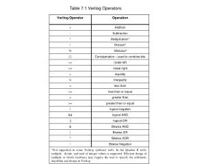
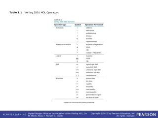
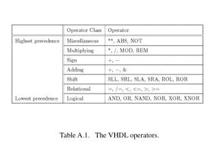
Table A.1. The VHDL operators. Figure A.1. The general structure of a VHDL design entity. Figure A.3. The general form of an architecture. Figure A.4. Code for a full-adder. Figure A.5. The general form of a PACKAGE declaration.

E N D
Figure A.7. Code for a four-bit adder, using component instantiation.
Figure A.8. Instantiating a four-bit adder from the LPM library.
Figure A.11. Code for a four-bit adder, using arithmetic expressions.
Figure A.12. A priority encoder described with a conditional signal assignment.
Figure A.23. A FOR-LOOP that does not represent a sensible circuit.
Figure A.24. The FOR-LOOP from Figure A.23 using a variable.
Figure A.25. The circuit generated from the code in Figure A.24.
Figure A.26. Using a variable to describe an n-input NAND gate.
Figure A.31. Equivalent code to Figure A.30, using a WAIT UNTIL statement.
Figure A.33. D flip-flop with synthronous reset, using an IF statement.
Figure A.34. D flip-flop with synchronous reset, using a WAIT UNTIL statement.
Figure A.35. Code for a four-bit register with asynchronous clear.
Figure A.36. Code for an n-bit register with asynchronous clear. Figure A.36. Code for an n-bit register with asynchronous clear.
Figure A.37. VHDL code for an n-bit register with an enable input.
Please see “portrait orientation” PowerPoint file for Chapter 10 Figure A.42. Component declarations for the accumulator circuit.
Please see “portrait orientation” PowerPoint file for Chapter 10 Figure A.43. Code for the accumulator circuit.
Please see “portrait orientation” PowerPoint file for Chapter 10 Figure A.45. An example of a Moore-type finite state machine.
Please see “portrait orientation” PowerPoint file for Chapter 10 Figure A.46. Code equivalent to Figure A.45, using two processes.
Please see “portrait orientation” PowerPoint file for Chapter 10 Figure A.48. An example of a Mealy-type Machine