Download
1 / 17
180 likes | 351 Views
Short Pulse Reading for STT-RAM. fren@ee.ucla.edu. Background. Ferro-magnetic layers. Anti-parallel. Parallel. Low R P - â€0â€. High R AP - â€1â€. STT-RAM Storage element: MTJ Represents “0/1†by the configuration of magnetization direction Read/Write operations: CMOS circuits

E N D
Short Pulse Reading for STT-RAM fren@ee.ucla.edu
Background Ferro-magnetic layers Anti-parallel Parallel Low RP - ”0” High RAP - ”1” • STT-RAM • Storage element: MTJ • Represents “0/1” by the configuration of magnetization direction • Read/Write operations: CMOS circuits • CMOS and MTJ variability are increasing • Resulting in more stringent constraints on CMOS design
Read Circuit Design Write (2) Short Pulse Reading (1) Low Current Reading Read • Sense the RMTJ (RAP / RP) through IREAD • Without disturbing the cell (0% switching prob.) • Two ways to get 0% switching probability • Low current reading (LCR) • Short pulse reading (SPR)
Read Circuit Design Write 2 ways to get 0% switching prob. (2) Short Pulse Reading (1) Low Current Reading Read • JC scaling will eventually create difficulty for LCR • How to implement SPR? • What is the circuit structure?
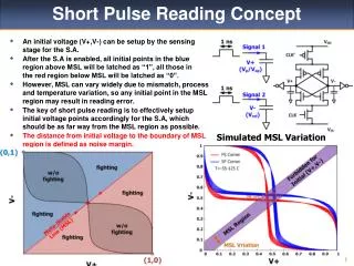
How to implement SPR? • When can we turn off sensing circuit? • When a safe read margin (VMTJ-VREF > VOS_latch + NM) is established • VOS_latch < 15 mV • How fast that read margin can be established? • The best SPR circuit should be able to establish the largest read margin with the least time.
#1: Current-Mirror Sense Amp (CMSA) [1] D. Gogl, et al., JSSC, Vol. 40, No. 4, Apr. 2005 [2] J.P. Kim, et al., VLSI, 2011 [3] J. Kim, et al., JVLSI, 2011 • Current Sensing • Speed is limited by the IMTJ • VMTJ is fixed, between VMTJ_P and VMTJ_AP • VMTJ-VREF is limited
#2: Split-Path Sense Amp (SPSA) [1] S.O. Jing, et al., US Patent, Pub. No. US 2010/0321976 A1 • Current Sensing • Speed is limited by the IMTJ • VMTJ is reverse to VMTJ • Larger VMTJ-VREF
#3: Body-Voltage Sense Amp (BVSA) • VMTJ is reverse to VMTJ • Even larger VMTJ-VREF • Benefiting from gain of the sense amp • Body Voltage Sensing • Body-connected load is better than diode connected load • Speed is no longer limited by IMTJ [My proposal]
RM Definition -3σ +3σ RMP RMAP RMP = μ(VMTJ,P − VREF,P) + 3σ(VMTJ,P − VREF,P) should be < 0 RMAP = μ(VMTJ,AP − VREF,AP) − 3σ(VMTJ,AP − VREF,AP) should be > 0
RM and performance Comparison Current sensing Voltage sensing We compare 3 sensing circuits at ISO reading current: • #1: Current-Mirror Sense Amp (CMSA) • Qualcomm design [VLSI’11] • #2: Split-Path Sense Amp (SPSA) • Qualcomm design [US Patent 2010/0321976 A1] • #3: Body-Voltage Sense Amp (BVSA) • UCLA proposal to demonstrate the read margin and speed advantage of our approach
Simulation Setup • MTJ • Size: 40x100 nm • RA = 9 Ω∙um2, TMR = 110%, Rp = 2.9 kΩ • Iread,P ~ 50 uA, Iread,ap ~ 30 uA • 5σ MTJ variation • 1 σRA = 4%, 1 σTMR = 5% • CMOS • 65-nm • Process Variation • Chip-to-chip + across chip local variation (ACLV) • Monte Carlo Run # = 5000 • Temp and VDD are kept the same in comparison • room temp • VDD = 1V
IMTJ Distribution CMSA SPSA BVSA
SMTJ − SREF Distribution SPSA BVSA
VMTJ and VREF Distribution CMSA SPSA BVSA After VMTJ and VREF are settled
VMTJ − VREF Distribution and RM CMSA SPSA BVSA After VMTJ and VREF are settled
RM vs. Sensing Time (Pulse Width) Sensing time (ns) required to achieve a given RM Write Read
Summary and Conclusions Methodology: • Proposed body-voltage sense amp (BVSA) reading circuit is compared with two existing current-sense reading circuits. Read margin and sensing time are compared at the same reading current. Observations: • Our circuit shows the biggest read margin • > 400 mV improvement as compared CMSA • > 250 mV improvement as compared to SPSA • Our circuit achieves high read margin with much shorter pulse width (sensing time)