Download
1 / 17
170 likes | 320 Views
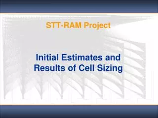
Towards An Early Design Space Exploration Tool Set for STT-RAM Design. Philip Asare and Ben Melton. STT-RAM Overview: Advantages. Everything volatile currently has High speed (SRAM) Density (DRAM) AND Everything non-volatile presents Non-volatility Low Power (Flash)

E N D
Towards An Early Design Space Exploration ToolSet for STT-RAM Design Philip Asare and Ben Melton
STT-RAM Overview: Advantages • Everything volatile currently has • High speed (SRAM) • Density (DRAM) • AND Everything non-volatile presents • Non-volatility • Low Power (Flash) • Reliability (Hard-drive) • On its own • CMOS-compatible • Good scalability potential (over tradition MRAM) • Potential for use as universal memory
STT-RAM Overview: Challenges • Device-Level • Tunneling Magneto-Resistance Ratio (TMR) • Fabrication Issues • Circuit-Level • Current-sensing • Variation • cell strength: reading difficulty • sense amp: offset (especially at smaller nodes) • Stochastic nature of MTJ • Architecture-Level • Read-write asymmetry in energy and delay • Periphery components may dominate
Road Map • STT-RAM Overview • Advantages • Challenges • Requirements for Addressing Challenges • Our Approach to Addressing Challenges • Understanding STT-RAM • Experimental Setup • Results + Insights • Future Work + Summary
Addressing STT-RAM Challenges • Requires cross-layer design • Layers of abstraction can get in the way • Need to know impact of decisions across layers • Need ‘generic’ way of doing this • Tools available for cross-layer design (from SRAM) • Technology Agnostic Simulation Environment (TASE) • Process-to-Circuit-Level Interface • One simulation template different PTMs • Virtual Prototyper (ViPro) • Circuit-to-Architecture-Level Interface • Circuit-level decisions on Arch-level and vice versa • Can work on TASE output to provide full cross-layer view • Our Approach: Extend TASE + ViPro Concept for STT-RAM
Understanding STT-RAM: Structures Storage Element* Array MTJ Resistance Characteristics* * A. Nigam et al., “Delivering on the Promise ofUniversal Memory for Spin Torque Transfer RAM (STT-RAM)” International Symposium on Low-Power Electronics and Design (ISLPED), August 2011 Bit Cell and Column
Understanding STT-RAM: Read Decode address select word Turn on sense amp pre-charge BL Disable precharge evaluate/read data Turn off sense amp X X (1) (2) (1) (1) X (2) (1) (2) (3) (4)
Understanding STT-RAM: Write Decode address select word Charge BL or SL to write (depends on value) Disable write transistors X or (2) (2) or X (1) (2) or X X or (2) (3) (1) (1) (2) (3)
Experimental Setup • Independent Variables • Process Level: Technology PTM • Circuit-Level: VDD, W (of access transistor) • Array-Level: Capacity, # Rows , Word size • Dependent Variables • Energy: Read and Write (FOM) • Delay: Read and Write (FOM) • Associated intermediate variables (e.g. bit cell write time)
Experimental Setup • Experimental Workflow • Simulations • TASE • For each PTM, vary VDD+W • Collect currents (read +write) • HSPICE • Collect sense amp info (current, delay, Vreadf(V)) • ViPro (Analytical Modeling and Virtual Prototyping) • use TASE output to calculate intermediate variables • compute FOMs based on analytical models
Results: Bit Cell Analysis • Setup • Iwrite-V Curve • General Results • Current increases with voltage • Current increases with node size
Results: Array-Level Decisions • Setup • Fixed Capacity (1MB) • Fixed VDD=0.9V, W=22nm (22nmPTM) • Varied #rows and word size • General Results • E, D write > read • D read ~ x1ns • D write ~ x10ns • E read, write < 1pJ • E, D more sensitive to wordsize
Results: Circuit-Level Decisions • Setup • Fixed array structure • Vary VDD and W (22nm PTM) • General Results • Energy increases with VDD • Delay decreases with increased VDD
Results: Circuit-Level Decisions • Setup • Fixed array capacity • Vary VDD and W (22nm PTM) • General Results • Width has little effect on energy
Results: Process-Level Decisions • Setup • Fixed array structure • Fix VDD=nominal for PTM, W=2Wmin • Vary PTM • General Results • PTM has more effect on energy • E,D increases with node size • *Note: write delay artifact of model
Insights • Majority of energy consumed in periphery • Decoders, Sense Amps • Cross-layer view better for optimization • Difficult to do without tools like TASE and ViPro • STT-RAM modeling and design is still in its infancy • Few good models available • Available models inconsistent from one to the other • Three distinct perspectives • Process, circuit, and architecture with nothing in between • Tough to reconcile perspectives
Future Work + Summary • Future • Improve STT-RAM Models!!! • Requires more research and understanding • We made a lot of assumptions • Extend tools for more comprehensive analysis • Integrate tools better (minor implementation issue) • We did a lot of manual ‘gluing’ • Summary • STT-RAM has the potential to shake the memory industry • Challenges in design need to be overcome • Cross-layer design perspective required • We showed this can be done