BCD to Excess-3 Converter: Implementation Strategies & Design Examples
Learn about ROM-based design, state transition tables, circuit realization, and timing behavior for BCD to Excess-3 Code conversion. Case study using Xilinx FPGAs.


BCD to Excess-3 Converter: Implementation Strategies & Design Examples
E N D
Presentation Transcript
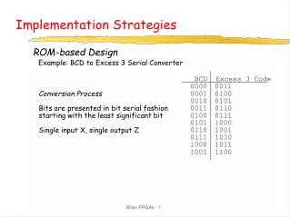
Implementation Strategies ROM-based Design Example: BCD to Excess 3 Serial Converter BCD Excess 3 Code 0000 0011 0001 0100 0010 0101 0011 0110 0100 0111 0101 1000 0110 1001 0111 1010 1000 1011 1001 1100 Conversion Process Bits are presented in bit serial fashion starting with the least significant bit Single input X, single output Z Xilinx FPGAs - 1
Implementation Strategies State Transition Table Derived State Diagram Xilinx FPGAs - 2
Implementation Strategies ROM-based Implementation Circuit Level Realization 74175 = 4 x positive edge triggered D FFs Truth Table/ROM I/Os In ROM-based designs, no need to consider state assignment Xilinx FPGAs - 3
Implementation Strategies LSB MSB Timing Behavior for input strings 0 0 0 0 (0) and 1 1 1 0 (7) 0 0 0 0 1 1 0 0 1 1 1 0 0 1 0 1 LSB LSB Xilinx FPGAs - 4
Implementation Strategies PLA-based Design State Assignment with NOVA S0 = 000 S1 = 001 S2 = 011 S3 = 110 S4 = 100 S5 = 111 S6 = 101 0 S0 S1 1 1 S0 S2 0 0 S1 S3 1 1 S1 S4 0 0 S2 S4 0 1 S2 S4 1 0 S3 S5 0 1 S3 S5 1 0 S4 S5 1 1 S4 S6 0 0 S5 S0 0 1 S5 S0 1 0 S6 S0 1 NOVA derived state assignment 9 product term implementation NOVA input file Xilinx FPGAs - 5
Implementation Strategies .i 4 .o 4 .ilb x q2 q1 q0 .ob d2 d1 d0 z .p 9 0001 0100 10-0 0100 01-0 0100 1-1- 0001 -0-1 1000 0-0- 0001 -1-0 1000 --10 0100 ---0 0010 .e .i 4 .o 4 .ilb x q2 q1 q0 .ob d2 d1 d0 z .p 16 0 000 001 1 1 000 011 0 0 001 110 1 1 001 100 0 0 011 100 0 1 011 100 1 0 110 111 0 1 110 111 1 0 100 111 1 1 100 101 0 0 111 000 0 1 111 000 1 0 101 000 1 1 101 --- - 0 010 --- - 1 010 --- - .e Espresso Inputs Espresso Outputs Xilinx FPGAs - 6
Implementation Strategies D2 = Q2 • Q0 + Q2 • Q0 D1 = X • Q2 • Q1 • Q0 + X • Q2 • Q0 + X • Q2 • Q0 + Q1 • Q0 D0 = Q0 Z = X• Q1 + X • Q1 Xilinx FPGAs - 7
Implementation Strategies 10H8 PAL: 10 inputs, 8 outputs, 2 product terms per OR gate D1 = D11 + D12 D11 = X • Q2 • Q1 • Q0 + X • Q2 • Q0 D12 = X • Q2 • Q0 + Q1 • Q0 0. Q2 • Q0 1. Q2 • Q0 8. X • Q2 • Q1 • Q0 9. X • Q2 • Q0 16. X • Q2 • Q0 17. Q1 • Q0 24. D11 25. D12 32. Q0 33. not used 40. X • Q1 41. X • Q1 Xilinx FPGAs - 8
Implementation Strategies Xilinx FPGAs - 9
Implementation Strategies Buffered Input or product term Registered PAL Architecture Negative Logic Feedback D2 = Q2 • Q0 + Q2 • Q0 D1 = X • Q2 • Q1 • Q0 + X • Q2 + X • Q0 + Q2 • Q0 + Q1 • Q0 D0 = Q0 Z = X • Q1 + X • Q1 Xilinx FPGAs - 10
Implementation Strategies Programmable Output Polarity/XOR PALs Buried Registers: decouple FF from the output pin Advantage of XOR PALs: Parity and Arithmetic Operations Xilinx FPGAs - 11
Implementation Strategies Example of XOR PAL Example of Registered PAL Xilinx FPGAs - 12
Specifying PALs with ABEL P10H8 PAL module bcd2excess3 title 'BCD to Excess 3 Code Converter State Machine' u1 device 'p10h8'; "Input Pins X,Q2,Q1,Q0,D11i,D12i pin 1,2,3,4,5,6; "Output Pins D2,D11o,D12o,D1,D0,Z pin 19,18,17,16,15,14; INSTATE = [Q2, Q1, Q0]; S0 = [0, 0, 0]; S1 = [0, 0, 1]; S2 = [0, 1, 1]; S3 = [1, 1, 0]; S4 = [1, 0, 0]; S5 = [1, 1, 1]; S6 = [1, 0, 1]; equations D2 = (!Q2 & Q0) # (Q2 & !Q0); D1 = D11i # D12i; D11o = (!X & !Q2 & !Q1 & Q0) # (X & !Q2 & !Q0); D12o = (!X & Q2 & !Q0) # (Q1 & !Q0); D0 = !Q0; Z = (X & Q1) # (!X & !Q1); end bcd2excess3; Explicit equations for partitioned output functions Xilinx FPGAs - 13
Specifying PALs with ABEL P12H6 PAL module bcd2excess3 title 'BCD to Excess 3 Code Converter State Machine' u1 device 'p12h6'; "Input Pins X, Q2, Q1, Q0 pin 1, 2, 3, 4; "Output Pins D2, D1, D0, Z pin 17, 18, 16, 15; INSTATE = [Q2, Q1, Q0]; OUTSTATE = [D2, D1, D0]; S0in = [0, 0, 0]; S0out = [0, 0, 0]; S1in = [0, 0, 1]; S1out = [0, 0, 1]; S2in = [0, 1, 1]; S2out = [0, 1, 1]; S3in = [1, 1, 0]; S3out = [1, 1, 0]; S4in = [1, 0, 0]; S4out = [1, 0, 0]; S5in = [1, 1, 1]; S5out = [1, 1, 1]; S6in = [1, 0, 1]; S6out = [1, 0, 1]; equations D2 = (!Q2 & Q0) # (Q2 & !Q0); D1 = (!X & !Q2 & !Q1 & Q0) # (X & !Q2 & !Q0) # (!X & Q2 & !Q0) # (Q1 & !Q0); D0 = !Q0; Z = (X & Q1) # (!X & !Q1); end bcd2excess3; Simpler equations Xilinx FPGAs - 14
Specifying PALs with ABEL P16R4 PAL module bcd2excess3 title 'BCD to Excess 3 Code Converter' u1 device 'p16r4'; "Input Pins Clk, Reset, X, !OE pin 1, 2, 3, 11; "Output Pins D2, D1, D0, Z pin 14, 15, 16, 13; SREG = [D2, D1, D0]; S0 = [0, 0, 0]; S1 = [0, 0, 1]; S2 = [0, 1, 1]; S3 = [1, 1, 0]; S4 = [1, 0, 0]; S5 = [1, 1, 1]; S6 = [1, 0, 1]; state_diagram SREG state S0: if Reset then S0 else if X then S2 with Z = 0 else S1 with Z = 1 state S1: if Reset then S0 else if X then S4 with Z = 0 else S3 with Z = 1 state S2: if Reset then S0 else if X then S4 with Z = 1 else S4 with Z = 0 state S3: if Reset then S0 else if X then S5 with Z = 1 else S5 with Z = 0 state S4: if Reset then S0 else if X then S6 with Z = 0 else S5 with Z = 1 state S5: if Reset then S0 else if X then S0 with Z = 1 else S0 with Z = 0 state S6: if Reset then S0 else if !X then S0 with Z = 1 end bcd2excess3; Xilinx FPGAs - 15
FSM Design with Counters Synchronous Counters: CLR, LD, CNT Four kinds of transitions for each state: (1) to State 0 (CLR) (2) to next state in sequence (CNT) (3) to arbitrary next state (LD) (4) loop in current state Careful state assignment is needed to reflect basic sequencing of the counter Xilinx FPGAs - 16
FSM Design with Counters Excess 3 Converter Revisited Note the sequential nature of the state assignments Xilinx FPGAs - 17
FSM Design with Counters Excess 3 Converter CLR signal dominates LD which dominates Count Xilinx FPGAs - 18
Implementing FSMs with Counters .i 5 .o 7 .ilb res x q2 q1 q0 .ob z clr ld en c b a .p 17 1---- -0----- 00000 1111--- 00001 1111--- 00010 0111--- 00011 00----- 00100 0111--- 00101 110-011 00110 10----- 00111 ------- 01000 010-100 01001 010-101 01010 1111--- 01011 10----- 01100 1111--- 01101 0111--- 01110 ------- 01111 ------- .e .i 5 .o 7 .ilb res x q2 q1 q0 .ob z clr ld en c b a .p 10 0-001 0101101 -0-01 1000000 -11-0 1000000 0-0-0 0101100 -000- 1010000 -0--0 0010000 0-10- 0101011 --11- 1000000 -11-- 0010000 -1-1- 1010000 .e Espresso Input File Excess 3 Converter Espresso Output File Xilinx FPGAs - 19
FSM Implementation with Counters Excess 3 Converter Schematic Synchronous Output Register Xilinx FPGAs - 20
Implementation Strategies Xilinx LCA Architecture Implementing the BCD to Excess 3 FSM Q2+ = Q2 • Q0 + Q2 • Q0 Q1+ = X • Q2 • Q1 • Q0 + X • Q2 • Q0 + X • Q2 • Q0 + Q1 • Q0 Q0+ = Q0 Z = Z • Q1 + X • Q1 No function more complex than 4 variables 4 FFs implies 2 CLBs Synchronous Mealy Machine Global Reset to be used Place Q2+, Q0+ in once CLB Q1, Z in second CLB maximize use of direct & general purpose interconnections Xilinx FPGAs - 21
Implementing the BCD to Excess 3 FSM Xilinx FPGAs - 22
Design Case Study Traffic Light Controller Decomposition into primitive subsystems • Controller FSM next state/output functions state register • Short time/long time interval counter • Car Sensor • Output Decoders and Traffic Lights Xilinx FPGAs - 23
Design Case Study Traffic Light Controller Block Diagram Xilinx FPGAs - 24
Design Case Study Subsystem Logic Light Decoders Car Detector Interval Timer Xilinx FPGAs - 25
Design Case Study State Assignment: HG = 00, HY = 10, FG = 01, FY = 11 P1 = C TL Q1 + TS Q1 Q0 + C Q1 Q0 + TS Q1 Q0 P0 = TS Q1 Q0 + Q1 Q0 + TS Q1 Q0 ST = C TL Q1 + C Q1 Q0 + TS Q1 Q0 + TS Q1 Q0 HL[1] = TS Q1 Q0 + Q1 Q0 + TS Q1 Q0 HL[0] = TS Q1 Q0 + TS Q1 Q0 FL[1] = Q0 FL[0] = TS Q1 Q0 + TS Q1 Q0 Next State Logic PAL/PLA Implementation: 5 inputs, 7 outputs, 8 product terms PAL 22V10 -- 11 inputs, 10 prog. IOs, 8 to 14 prod terms per OR ROM Implementation: 32 word by 8-bit ROM (256 bits) Reset may double ROM size Xilinx FPGAs - 26
Design Case Study Counter-based Implementation 2 x 4:1 MUX TTL Implementation with MUX and Counter Can we reduce package count by using an 8:1 MUX? Xilinx FPGAs - 27 ST = Count
Design Case Study Counter-based Implementation Dispense with direct output functions for the traffic lights Why not simply decode from the current state? ST is a Synchronous Mealy Output Light Controllers are Moore Outputs Xilinx FPGAs - 28
Design Case Study LCA-Based Implementation Discrete Gate Method: None of the functions exceed 5 variables P1, ST are 5 variable (1 CLB each) P0, HL1, HL0, FL0 are 3 variable (1/2 CLB each) FL1 is 1 variable (1/2 CLB) 4 1/2 CLBs total! Xilinx FPGAs - 29
Design Case Study LCA-Based Implementation Placement of functions selected to maximize the use of direct connections Xilinx FPGAs - 30
Design Case Study LCA-Based Implementation Counter/Multiplexer Method: 4:1 MUX, 2 Bit Upcounter MUX: six variables (4 data, 2 control) but this is the kind of 6 variable function that can be implemented in 1 CLB! 2nd CLB to implement TL • C and TL + C' But note that ST/Cnt is really a function of TL, C, TS, Q1, Q0 1 CLB to implement this function of 5 variables! 2 Bit Counter: 2 functions of 3 variables (2 bit state + count) Also implemented in one CLB Traffic light decoders: functions of 2 variables (Q1, Q0) 2 per CLB = 3 CLB for the six lights Total count = 5 CLBs Xilinx FPGAs - 31