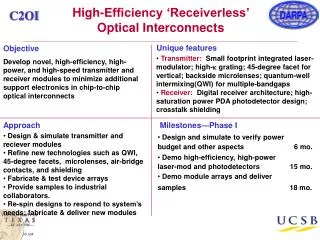
High-Efficiency ‘Receiverless’ Optical Interconnects
High-Efficiency ‘Receiverless’ Optical Interconnects. Unique features. Objective. Transmitter: Small footprint integrated laser-modulator; high- k grating; 45-degree facet for vertical; backside microlenses; quantum-well intermixing(QWI) for multiple-bandgaps

High-Efficiency ‘Receiverless’ Optical Interconnects
E N D
Presentation Transcript
High-Efficiency ‘Receiverless’ Optical Interconnects Unique features Objective • Transmitter: Small footprint integrated laser-modulator; high-k grating; 45-degree facet for vertical; backside microlenses; quantum-well intermixing(QWI) for multiple-bandgaps • Receiver: Digital receiver architecture; high-saturation power PDA photodetector design; crosstalk shielding Develop novel, high-efficiency, high-power, and high-speed transmitter and receiver modules to minimize additional support electronics in chip-to-chip optical interconnects Approach Milestones—Phase I • Design & simulate transmitter and reciever modules • Refine new technologies such as QWI, 45-degree facets, microlenses, air-bridge contacts, and shielding • Fabricate & test device arrays • Provide samples to industrial collaborators. • Re-spin designs to respond to system’s needs; fabricate & deliver new modules • Design and simulate to verify power • budget and other aspects 6 mo. • Demo high-efficiency, high-power • laser-mod and photodetectors 15 mo. • Demo module arrays and deliver • samples 18 mo.
Criteria/Concepts Criteria • Support data rates up to 40 Gbs • Small footprint and low power dissipation Concepts • Avoid additional driver/receiver electronics • Use integrated in-plane laser-modulator at ~ 980 nm to get bandwidth and power required at high efficiency • Use high saturation power photodetector to directly drive logic (or same Si receiver as used for electrical interconnects)
Technical Approach: Transmitter • Design & simulate short cavity laser, high-coupling gratings, and shallow-quantum-well modulator sections. Insure power budget is satisfied and thermal issues are understood. • Refine QWI to simultaneously optimize gain, grating and EAM sections • Fabricate & test device arrays • Re-spin designs to respond to system’s needs, fabricate & deliver new modules to industrial collaborators. • In Phase II develop 45-degree facets and, microlenses for collimated vertical emission IPSEL-Mod Longitudinal cross sections End-on view
Technical Approach: Receiver PDA Bandstructure • Design & simulate partially-depleted absorber photodetector for optical interconnect applications. Insure ‘digital receiver’ architecture is valid and that power budget is satisfied. • Refine PDA-PD design and secure wafers. • Fabricate & test device arrays • Re-spin designs to respond to system’s needs, fabricate & deliver new modules to industrial collaborators. • In Phase II further develop crosstalk shields, air bridge contacts, and other necessary improvements to meet specifications. Air-bridge contacts Initial results
Threshold current and temperature rise vs. Lg Active length: 75 μm Rear DBR length: 40 μm Ridge width: 2 μm Kappa: 650 cm-1 Grating etch depth: 480Å LASER Simulation
Optical Receiver Options Conventional Receiver Design “Amplifierless” Receiver Design Lower noise Higher speed PIN Photodiode High saturation power High speed (High linearity)