Agenda
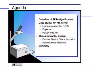
Agenda. Overview of RF Design Process Case study: RF Front-end Low-noise amplifier (LNA) Duplexer Power amplifier Measurement for Design Passive Device Characterization Active Device Modeling Summary. Physical. Design. Integrate. Redesign. Build. Test. NO. Does it work?.

Agenda
E N D
Presentation Transcript
Agenda • Overview of RF Design Process • Case study: RF Front-end • Low-noise amplifier (LNA) • Duplexer • Power amplifier • Measurement for Design • Passive Device Characterization • Active Device Modeling • Summary
Physical Design Integrate Redesign Build Test NO Does it work? Production The Traditional Non-Predictive Design Process Concept Design Integrate Production
Design Integrate Software Simulate Redesign Does it work? NO Manufacturable ? NO Build Test NO Does it work? Physical Production The Predictive RF Design Process Concept • Adjust the design on the work station not on the bench! Design Integrate Production
HP Advanced Design System Total integration of schematic, simulation, and layout
Concept: System-Level Design(Simple PCS-band transceiver front end) Power Amp Freq. = 1880 MHz +/- 50 MHz min. Pout (1 dB) = +27 dBm min Psat = +30 dBm min Gain = 25 dB min 1.9 GHz Duplexer Freq. lower band = 1880 MHz +/- 30 MHz Freq. upper band = 1960 MHz +/- 30 MHz LNA Freq. = 1960 MHz +/- 50 MHz min. Gain = 25 dB min NF < 3 dB The first part of the case study will focus on the LNA
This one’s good! But...What about Yield? Volume Performance Variation Individual Performance Optimized Performance (Gain, dB) Performance (Gain, dB) Tolerance Range Tolerance Range Design Spec Component Value (Cload, pF) Component Value (Cload, pF)
Working Power Amplifier !!! Measured Simulated
CDMA Tests Channel Power and ACPR Simulation Measured Pwr = 11.2 dBm Pwr = 10.8 dBm ACPR < -70 dBc ACPR < -70 dBc
Typical PCB Fixture (with Cal Standards) Short standard Load standard Contact to DUT Open standard Launches / Transitions Thru standard Coaxial connectors
Thank You for Attending - HP RF Design and Measurement Seminar Authors: David Ballo Joe Civello Ed Henicle Sara Meszaros Andy Potter Boyd Shaw My Le Truong

