Download
1 / 17
210 likes | 401 Views
ECE/CS 252, Fall 2010 Prof. Mikko Lipasti Department of Electrical and Computer Engineering University of Wisconsin – Madison. Latches, Flip Flops, and Memory. Building Functions from Logic Gates.

E N D
ECE/CS 252, Fall 2010 Prof. Mikko Lipasti Department of Electrical and Computer Engineering University of Wisconsin – Madison Latches, Flip Flops, and Memory
Building Functions from Logic Gates We've already seen how to implement truth tablesusing AND, OR, and NOT, etc. -- examples of combinational logic. Combinational Logic Circuit • output depends only on the current inputs • stateless Sequential Logic Circuit • output depends on the sequence of inputs (past and present) • stores information (state) from past inputs Next we’ll show how to build sequential circuits that store information.
Combinational vs. Sequential Combinational Circuit • always gives the same output for a given set of inputs • ex: adder always generates sum and carry,regardless of previous inputs Sequential Circuit • stores information • output depends on stored information (state) plus input • so a given input might produce different outputs,depending on the stored information • example: ticket counter • advances when you push the button • output depends on previous state • useful for building “memory” elements and “state machines” Need a storage element
Storage is based on feedback Feedback – output is fed back to the input What if we add feedback to a pair of inverters? Usually drawn as a ring or cross-coupled inverters: Stable way to store one bit of information 0 1 0 0 1 0 1
Storage based on feedback How can we change the value that is stored? 1 0 1 “Set” A B Result: RS latch 0 “Set” “Reset” 1 0
R-S Latch: Simple Storage Element R is used to “reset” or “clear” the element – set it to zero. S is used to “set” the element – set it to one. If both R and S are one, out could be either zero or one. • “quiescent” state -- holds its previous value • note: if a is 1, b is 0, and vice versa 1 1 0 1 1 0 1 0 1 1 0 0 1 1
R-S Latch Summary R = S = 1 • hold current value in latch S = 0, R=1 • set value to 1 R = 0, S = 1 • set value to 0 R = S = 0 • both outputs equal one • final state determined by electrical properties of gates • Don’t do it! Correct use is a bit tricky, so …
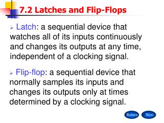
Gated D-Latch Two inputs: D (data) and WE (write enable) • when WE = 1, latch is set to value of D • S = NOT(D), R = D • when WE = 0, latch holds previous value • S = R = 1
• • • Memory Now that we know how to store bits,we can build a memory – a logical k × m array of stored bits. Address Space: number of locations(usually a power of 2) k = 2n locations Addressability: number of bits per location(e.g., byte-addressable) m bits
Example: 22 x 3 Memory word WE word select input bits address write enable address decoder output bits
More Memory Details This is a not the way actual memory is implemented. • fewer transistors and wires, much more dense, relies on electrical properties But the logical structure is very similar. • address decoder • word select line • word write enable Two basic kinds of RAM (Random Access Memory) Static RAM (SRAM) • fast, not very dense (bitcell is a latch) Dynamic RAM (DRAM) • slower but denser, bit storage must be periodically refreshed • each bitcell is a capacitor (like a leaky bucket) that decays Also, non-volatile memories: ROM, PROM, flash, …
Real SRAM Memory Memory Data In Write bitlines m Read Address Decoder . . . WE D D D Memory Read Address Write Address Decoder Read word line . . . D D D Memory WriteAddress n . . . Write word line . . . n . . . . . . D D D Gated D-latch D Q WE Read bitlines m Memory Data Out
Review: The Clock A clock circuit triggers transition fromone state to the next. At the beginning of each clock cycle,state machine makes a transition,based on the current state and the external inputs. “1” “0” One Cycle time
Sequential Circuits Combinational logic • Determine outputs and next state. Storage elements • Maintain state representation using … D latches? Clock is used to control WE of D latch • Clock is high => D input propagates to output • Then loops through combinational logic back to D input • Feedback cycle: big no-no for combinational circuits! • Have to make sure delay is longer than time that clock is high • Known as min-delay or shortest path constraint • Painful, difficult to get right, cannot slow clock down to debug “1” “0” State Machine Inputs Outputs Combinational Logic Circuit Storage Elements Clock
Instead: Master-Slave Flip-flop A pair of gated D-latches, to isolate next state from current state. During 1st phase (clock=1),previously-computed statebecomes current state and issent to the logic circuit. During 2nd phase (clock=0),next state, computed bylogic circuit, is stored inLatch A (master).
Master/Slave Flip-flop Two latches have opposite WE polarity from clock • As clock transitions from 0 to 1, master latch closes, slave latch opens • As clock transitions from 1 to 0, slave latch closes, master latch opens Flip-flop input is “copied” at the 0 to 1 transition or “edge” • There is only a brief window of time where both latches are open (could even be zero, if designed that way) • Closes the feedback loop • Enables simple reasoning about correctness • Short-path problem much easier (trivial, usually) • Can slow clock down arbitrarily Hereafter, assume MSFF-based sequential circuits
Summary Sequential circuits have state • Need a storage element to remember state RS Latch D Latch Memory Clocking issue with latch-based design D Master/Slave Flip-flop