Download
1 / 42
420 likes | 658 Views
Lecture 10 Registers, Counters and Shifters. Prith Banerjee ECE C03 Advanced Digital Design Spring 1998. Outline. Registers Register Files Counters Designs of Counters with various FFs Shifters READING: Katz 7.1, 7.2, 7.4, 7.5, 4.7 Dewey 10.2, 10.3, 10.4, Hennessy-Patterson B26.

E N D
Lecture 10 Registers, Counters and Shifters Prith Banerjee ECE C03 Advanced Digital Design Spring 1998 ECE C03 Lecture 10
Outline • Registers • Register Files • Counters • Designs of Counters with various FFs • Shifters • READING: Katz 7.1, 7.2, 7.4, 7.5, 4.7 Dewey 10.2, 10.3, 10.4, Hennessy-Patterson B26 ECE C03 Lecture 10
Building Complex Memory Elements • Flipflops: most primitive "packaged" sequential circuits • More complex sequential building blocks: Storage registers, Shift registers, Counters Available as components in the TTL Catalog • How to represent and design simple sequential circuits: counters • Problems and pitfalls when working with counters: Start-up States Asynchronous vs. Synchronous logic ECE C03 Lecture 10
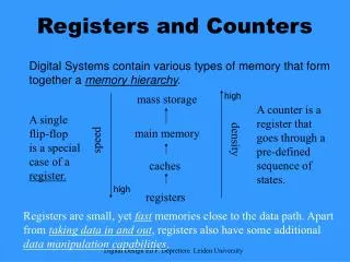
Registers • Storage unit. Can hold an n-bit value • Composed of a group of n flip-flops • Each flip-flop stores 1 bit of information • Normally use D flip-flops D Q Dff clk D Q Dff clk D Q Dff clk D Q Dff clk ECE C03 Lecture 10
Controlled Register D Q Dff clk D Q Dff clk D Q Dff clk D Q Dff clk ECE C03 Lecture 10
Registers Group of storage elements read/written as a unit 4-bit register constructed from 4 D FFs Shared clock and clear lines Schematic Shape TTL 74171 Quad D-type FF with Clear (Small numbers represent pin #s on package) ECE C03 Lecture 10
Variations of Registers Selective Load Capability Tri-state or Open Collector Outputs True and Complementary Outputs 74377 Octal D-type FFs with input enable 74374 Octal D-type FFs with output enable EN enabled low and lo-to-hi clock transition to load new data into register OE asserted low presents FF state to output pins; otherwise high impedence ECE C03 Lecture 10
Register Files Two dimensional array of flipflops Address used as index to a particular word Word contents read or written Separate Read and Write Enables Separate Read and Write Address Data Input, Q Outputs Contains 16 D-ffs, organized as four rows (words) of four elements (bits) 74670 4x4 Register File with Tri-state Outputs ECE C03 Lecture 10
Shift Registers Storage + ability to circulate data among storage elements \Reset Shift Direction J K Q Q J K Q Q Q Q J K Q Q J K Shift \Reset Shift Shift from left storage element to right neighbor on every lo-to-hi transition on shift signal Wrap around from rightmost element to leftmost element Q1 Q2 Q3 Q4 Master Slave FFs: sample inputs while clock is high; change outputs on falling edge ECE C03 Lecture 10
Shift Registers I/O Serial vs. Parallel Inputs Serial vs. Parallel Outputs Shift Direction: Left vs. Right Serial Inputs: LSI, RSI Parallel Inputs: D, C, B, A Parallel Outputs: QD, QC, QB, QA Clear Signal Positive Edge Triggered Devices S1,S0 determine the shift function S1 = 1, S0 = 1: Load on rising clk edge synchronous load S1 = 1, S0 = 0: shift left on rising clk edge LSI replaces element D S1 = 0, S0 = 1: shift right on rising clk edge RSI replaces element A S1 = 0, S0 = 0: hold state Multiplexing logic on input to each FF! QD QC QB QA 74194 4-bit Universal Shift Register Shifters well suited for serial-to-parallel conversions, such as terminal to computer communications ECE C03 Lecture 10
Application of Shift Registers Parallel to Serial Conversion Sender Receiver S1 S1 194 194 S0 S0 LSI LSI D D7 D D7 QD QD C D6 C D6 QC QC B D5 B D5 QB QB D4 A D4 A QA QA RSI RSI Clock CLK CLK Parallel Inputs Parallel Outputs CLR CLR S1 S1 194 194 S0 S0 LSI LSI D D3 D D3 QD QD C D2 C D2 QC QC B D1 B D1 QB QB D0 A D0 A QA QA RSI RSI CLK CLK CLR CLR Serial transmission ECE C03 Lecture 10
Counters Proceed through a well-defined sequence of states in response to count signal 3 Bit Up-counter: 000, 001, 010, 011, 100, 101, 110, 111, 000, ... 3 Bit Down-counter: 111, 110, 101, 100, 011, 010, 001, 000, 111, ... Binary vs. BCD vs. Gray Code Counters A counter is a "degenerate" finite state machine/sequential circuit where the state is the only output ECE C03 Lecture 10
Johnson Counters Q Q Q Q 1 2 3 4 Q 1 Q 2 Q 3 Q 4 + + + \Reset 1 0 End-Around S S S S J J J J Q Q Q Q CLK CLK CLK CLK K Q K Q K Q K Q R R R R Shift + 100 Shift 1 1 1 1 0 0 0 0 0 1 1 1 1 0 0 0 0 0 1 1 1 1 0 0 0 0 0 1 1 1 1 0 8 possible states, single bit change per state, useful for avoiding glitches ECE C03 Lecture 10
Catalog Counters 7 P 163 10 T 15 Synchronous Load and Clear Inputs Positive Edge Triggered FFs Parallel Load Data from D, C, B, A P, T Enable Inputs: both must be asserted to enable counting RCO: asserted when counter enters its highest state 1111, used for cascading counters "Ripple Carry Output" RCO 2 CLK 11 6 D QD 5 12 C QC 4 13 B QB 3 14 A QA 9 LOAD 1 CLR 74163 Synchronous 4-Bit Upcounter 74161: similar in function, asynchronous load and reset ECE C03 Lecture 10
74163 Detailed Timing Diagram Q A Q B Q C Q D CLR LOAD A B C D CLK P T RCO ECE C03 Lecture 10 12 13 14 15 0 1 2 Clear Load Count Inhibit
Counter Design Procedure This procedure can be generalized to implement ANY finite state machine Counters are a very simple way to start: no decisions on what state to advance to next current state is the output Example: 3-bit Binary Upcounter Present State Next State Flipflop Inputs 000 Decide to implement with Toggle Flipflops What inputs must be presented to the T FFs to get them to change to the desired state bit? This is called "Remapping the Next State Function" C B A C+ B+ A+ TC TB TA 0 0 0 0 0 1 0 0 1 0 0 1 0 1 0 0 1 1 0 1 0 0 1 1 0 0 1 0 1 1 1 0 0 1 1 1 1 0 0 1 0 1 0 0 1 1 0 1 1 1 0 0 1 1 1 1 0 1 1 1 0 0 1 1 1 1 0 0 0 1 1 1 001 State Transition Table Flipflop Input Table ECE C03 Lecture 10
Example Design of Counter K-maps for Toggle Inputs: Resulting Logic Circuit: CB 11 A 00 01 10 0 1 TA = CB 11 A 00 01 10 0 1 TB = CB 11 A 00 01 10 0 1 ECE C03 Lecture 10 TC =
Resultant Circuit for Counter Resulting Logic Circuit: K-maps for Toggle Inputs: + QA QB QC S S S Q Q Q T T T CLK CLK Q CLK Q Q R R R \Reset Count Timing Diagram: ECE C03 Lecture 10
More Complex Counter Design Step 1: Derive the State Transition Diagram Count sequence: 000, 010, 011, 101, 110 Present State Next State Step 2: State Transition Table 0 0 0 0 1 0 0 1 0 0 1 1 0 1 1 1 0 1 1 0 1 1 1 0 1 1 0 0 0 0 ECE C03 Lecture 10
Complex Counter Design (Contd) Step 1: Derive the State Transition Diagram Count sequence: 000, 010, 011, 101, 110 Present State Next State Step 2: State Transition Table 0 0 0 0 1 0 0 0 1 X X X 0 1 0 0 1 1 0 1 1 1 0 1 1 0 0 X X X 1 0 1 1 1 0 1 1 0 0 0 0 1 1 1 X X X Note the Don't Care conditions ECE C03 Lecture 10
Counter Design (Contd) Step 3: K-Maps for Next State Functions CB CB 11 A 00 01 10 11 A 00 01 10 0 0 1 1 C+ = B+ = CB 11 A 00 01 10 0 1 A+ = ECE C03 Lecture 10
Counter Design (contd) Step 4: Choose Flipflop Type for Implementation Use Excitation Table to Remap Next State Functions Present State Toggle Inputs C B A TC TB TA Q Q+ T 0 0 0 0 1 1 1 0 1 1 1 0 0 0 0 0 1 0 0 0 1 X X X 0 1 0 0 0 1 0 1 1 1 1 0 1 0 0 X X X 1 0 1 0 1 1 1 1 0 1 1 0 1 1 1 X X X Toggle Excitation Table Remapped Next State Functions ECE C03 Lecture 10
Resultant Counter Design Remapped K-Maps CB CB 11 A 00 01 10 11 A 00 01 10 0 0 1 1 TC TB CB 11 A 00 01 10 0 1 TA TC = A C + A C = A xor C TB = A + B + C TA = A B C + B C ECE C03 Lecture 10
Resultant Circuit for Complex Counter Resulting Logic: 5 Gates 13 Input Literals + Flipflop connections TB B TA A TC C S S S Q Q T Q T T Q Q Q CLK CLK CLK \C \B \A R R R Count \Reset A C \A B C \B C TC TA A \B C TB Timing Waveform: ECE C03 Lecture 10
Implementing Counters with Different FFs • Different counters can be implemented best with different counters • Steps in building a counter • Build state diagram • Build state transition table • Build next state K-map • Implementing the next state function with different FFs • Toggle flip flops best for binary counters • Existing CAD software for finite state machines favor D FFs ECE C03 Lecture 10
Implementing 5-state counter with RS FFs Continuing with the 000, 010, 011, 101, 110, 000, ... counter example Rmepped next state Present State Next State Q Q+ R S 0 0 X 0 0 1 0 1 1 0 1 0 1 1 0 X RC SC RB SB RA SA 0 0 0 0 1 0 X 0 0 1 X 0 0 0 1 X X X X X X X X X 0 1 0 0 1 1 X 0 0 X 0 1 0 1 1 1 0 1 0 1 1 0 0 X 1 0 0 X X X X X X X X X 1 0 1 1 1 0 0 X 0 1 1 0 1 1 0 0 0 0 1 0 1 0 X 0 1 1 1 X X X X X X X X X Q+ = S + R Q RS Exitation Table Remapped Next State Functions ECE C03 Lecture 10
Implementation with RS FFs CB CB 11 11 A 00 01 10 A 00 01 10 0 0 1 1 RC SC CB CB 11 11 A 00 01 10 A 00 01 10 0 0 1 1 RB SB CB CB 11 11 A 00 01 10 A 00 01 10 0 0 1 1 RA SA RS FFs Continued 0 0 0 X X 1 X X X X 1 X X 0 X 0 RC = A SC = A RB = A B + B C SB = B RA = C SA = B C 0 0 1 X X 1 X 0 1 X 0 X X 0 X 1 X 0 X X X 0 X 1 0 1 0 X X X X 0 ECE C03 Lecture 10
Implementation With RS FFs \ A \ B \ C \ B C B A RB R C R Q R Q Q CLK CLK CLK Q A S Q Q S SA S \A Count A B RB SA C B \C Resulting Logic Level Implementation: 3 Gates, 11 Input Literals + Flipflop connections ECE C03 Lecture 10
Implementing with JK FFs Continuing with the 000, 010, 011, 101, 110, 000, ... counter example Rmepped next state Present State Next State Q Q+ J K 0 0 0 X 0 1 1 X 1 0 X 1 1 1 X 0 JC KC JB KB JA KA 0 0 0 0 1 0 0 X 1 X 0 X 0 0 1 X X X X X X X X X 0 1 0 0 1 1 0 X X 0 1 X 0 1 1 1 0 1 1 X X 1 X 0 1 0 0 X X X X X X X X X 1 0 1 1 1 0 X 0 1 X X 1 1 1 0 0 0 0 X 1 X 1 0 X 1 1 1 X X X X X X X X X Q+ = S + R Q RS Exitation Table Remapped Next State Functions ECE C03 Lecture 10
Implementation with JK FFs CB CB 11 11 A 00 01 10 A 00 01 10 0 0 1 1 JC = A KC = A/ JB = 1 KB = A + C JA = B C/ KA = C JC KC CB CB 11 11 A 00 01 10 A 00 01 10 0 0 1 1 JB KB CB CB 11 11 A 00 01 10 A 00 01 10 0 0 1 1 JA KA ECE C03 Lecture 10
Implementation with JK FFs \ A \ C \ B \ A \ C + C B A A J Q J Q JA J Q CLK CLK CLK C K Q KB K Q K Q Count A B JA KB C Resulting Logic Level Implementation: 2 Gates, 10 Input Literals + Flipflop Connections ECE C03 Lecture 10
Implementation with D FFs Simplest Design Procedure: No remapping needed! DC = A DB = A C + B DA = B C Resulting Logic Level Implementation: 3 Gates, 8 Input Literals + Flipflop connections ECE C03 Lecture 10
Comparison with Different FF Types • T FFs well suited for straightforward binary counters But yielded worst gate and literal count for this example! • No reason to choose R-S over J-K FFs: it is a proper subset of J-K R-S FFs don't really exist anyway J-K FFs yielded lowest gate count Tend to yield best choice for packaged logic where gate count is key • D FFs yield simplest design procedure Best literal count D storage devices very transistor efficient in VLSI Best choice where area/literal count is the key ECE C03 Lecture 10
Asynchronous vs. Synchronous Counters Deceptively attractive alternative to synchronous design style Ripple Counters T Q T Q T Q A B C CLK Q CLK Q CLK Q Count Count signal ripples from left to right Count Reset A B C State transitions are not sharp! Can lead to "spiked outputs" from combinational logic decoding the counter's state ECE C03 Lecture 10
Power of Synchronous Clear and Load Starting Offset Counters: e.g., 0110, 0111, 1000, 1001, 1010, 1011, 1100, 1101, 1111, 0110, ... D C B A R Q Q Q Q 1 C D C B A L 6 C O O C 3 L A L K P T D C B A D R 0 1 + + Load Use RCO signal to trigger Load of a new state Since 74163 Load is synchronous, state changes only on the next rising clock edge 0110 is the state to be loaded ECE C03 Lecture 10
Shifters • We have discussed some core logic design circuits for designing datapaths of computers • adders • ALUs • multipliers • A final component which is very important is a shifter • Takes a n-bit input and performs a shift left or right by m bits • Can define arithmetic shifts, logical shifts or circular shifts, e.g. circular shift left a7 a6 a5 a4 a3 a2 a1 a0 a6 a5 a4 a3 a2 a1 a0 a7 ECE C03 Lecture 10
8-input Barrel Shifter Specification: Inputs: D7, D6, …, D0 Outputs: O7, O6, …, O0 Control: S2, S1, S0 shift input the specified number of positions to the right Understand the problem: D7 D6 D5 D4 D3 D2 D1 D0 O7 O6 O5 O4 O3 O2 O1 O0 D7 D6 D5 D4 D3 D2 D1 D0 O7 O6 O5 O4 O3 O2 O1 O0 D7 D6 D5 D4 D3 D2 D1 D0 O7 O6 O5 O4 O3 O2 O1 O0 . . . . . . . . . S2, S1, S0 = 0 0 1 S2, S1, S0 = 0 0 0 S2, S1, S0 = 0 1 0 ECE C03 Lecture 10
Functional Description of Shifter Function Table Boolean equations O7 = S2' S1' S0' D7 + S2' S1' S0 D6 + … + S2 S1 S0 D0 O6 = S2' S1' S0' D6 + S2' S1' S0 D5 + … + S2 S1 S0 D7 O5 = S2' S1' S0' D5 + S2' S1' S0 D4 + … + S2 S1 S0 D6 O4 = S2' S1' S0' D4 + S2' S1' S0 D3 + … + S2 S1 S0 D5 O3 = S2' S1' S0' D3 + S2' S1' S0 D2 + … + S2 S1 S0 D4 O2 = S2' S1' S0' D2 + S2' S1' S0 D1 + … + S2 S1 S0 D3 O1 = S2' S1' S0' D1 + S2' S1' S0 D0 + … + S2 S1 S0 D2 O0 = S2' S1' S0' D0 + S2' S1' S0 D7 + … + S2 S1 S0 D1 ECE C03 Lecture 10
8-input Barrel Shifter • Straightforward gate level implementation • Looking at the Boolean equations earlier it is not possible to simplify them • Discrete gate implementation would require • eight 4-input AND gates and one 8-input OR gate per outputfunction • total 64 8-input AND gates, and 8 8-input OR gates for 8 output functions • Requires 40 TTL SSI packages ECE C03 Lecture 10
Alternative Implementations of Shifter • Use MSI components such as multiplexers and decoders • Each output function can be implemented by an 8:1 multiplexer, need eight MUXex, eight packages • Use the control input S2 S1 S0 to control mux D7 D6 … D1 D0 D7 D6 … D1 D0 D7 D6 … D1 D0 O0 O6 O7 S2S1S0 S2S1S0 S2S1S0 ECE C03 Lecture 10
Shifter Design Using Switching Logic • Remember that one can use CMOS transistors as switches • that turn on when the gate signal is high, and off when gate • signal is low • Need 64 switches (transistors) plus a decoder in a regular design Crosspoint switches Fully Wired crosspoint switch ECE C03 Lecture 10
Summary • Registers • Register Files • Counters • Designs of Counters with various FFs • Shifters • NEXT LECTURE: Memory Design • READING: Katz 7.6 ECE C03 Lecture 10