Registers and Counters
Registers and Counters. Chapter 6. 6.1 Registers. Clocked sequential circuits a group of flip-flops and combinational gates connected to form a feedback path Flip-flops + Combinational gates (essential) (optional) Register: a group of flip-flops

Registers and Counters
E N D
Presentation Transcript
Registers and Counters Chapter 6
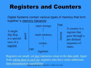
6.1 Registers • Clocked sequential circuits • a group of flip-flops and combinational gates • connected to form a feedback path Flip-flops + Combinational gates (essential) (optional) • Register: • a group of flip-flops • gates that determine how the information is transferred into the register • Counter: • a register that goes through a predetermined sequence of states
6-1 Registers • A n-bit register • n flip-flops capable of storing n bits of binary information • 4-bit register Fig. 6.1 Four-bit register
load' • 4-bit register with parallel load load Fig. 6.2 Four-bit register with parallel load
6-2 Shift Registers • Shift register • a register capable of shifting its binary information in one or both directions • Simplest shift register 0 0 1 1 1 1 1 1 0 1 Fig. 6.3 Four-bit shift register
Serial transfer vs. Parallel transfer • Serial transfer • Information is transferred one bit at a time • shifts the bits out of the source register into the destination register • Parallel transfer: • All the bits of the register are transferred at the same time
Example: Serial transfer from reg A to reg B Fig. 6.4 Serial transfer from register A to register B
Serial addition using D flip-flops 1 0 0 0 0101 1010 1 1 0 1 1 1 0011 ?001 Fig. 6.5 Serial adder
Serial adder using JK flip-flops JQ = x y KQ = x y = (x + y) S = x y Q
Circuit diagram JQ = x y KQ = x y = (x + y) S = x y Q Ci Fig. 6.6 Second form of serial adder
Universal Shift Register • Unidirectional shift register • Bidirectional shift register • Universal shift register: • has both direction shifts & parallel load/out capabilities
Capability of a universal shift register: • A clear control to clear the register to 0. • A clock input to synchronize the operations. • A shift-right control to enable the shift right operation and the serial input and output lines associated w/ the shift right. • A shift-left control to enable the shift left operation and the serial input and output lines associated w/ the shift left. • A parallel-load control to enable a parallel transfer and the nparallel input lines associated w/ the parallel transfer. • nparallel output lines. • A control state that leaves the information in the register unchanged in the presence of the clock.
Example: 4-bit universal shift register Fig. 6.7 Four-bit universal shift register
Function table Clear s1 s0A3+ A2+ A1+ A0+(operation) 0 × × 0 0 0 0 Clear 1 0 0A3 A2 A1 A0 No change 1 0 1 sri A3 A2 A1Shift right 1 1 0 A2 A1 A0sliShift left 1 1 1 I3 I2 I1 I0Parallel load 第三版內容,參考用!
A0 A1 A2 Fig. 6.7 Four-bit universal shift register (continued)
6-3 Ripple Counters • Counter: • a register that goes through a prescribed sequence of states • upon the application of input pulses • Input pulses: may be clock pulses or originate from some external source • The sequence of states: may follow the binary number sequence ( Binary counter) or any other sequence of states
Categories of counters • Ripple counters The flip-flop output transition serves as a source for triggering other flip-flops no common clock pulse (not synchronous) • Synchronous counters: The CLK inputs of all flip-flops receive a common clock
Example: 4-bit binary ripple counter • Binary count sequence: 4-bit
10 10 Fig. 6.8 Four-bit binary ripple counter
BCD ripple counter Fig. 6.9 State diagram of a decimal BCD counter
The circuit Fig. 6.10 BCD ripple counter
Three-decade BCD counter Fig. 6.11 Block diagram of a three-decade decimal BCD counter
6-4 Synchronous Counters • Sync counter • A common clock triggers all flip-flops simultaneously • Design procedure • apply the same procedure of sync seq ckts • Sync counter is simpler than general sync seq ckts
4-bit binary counter C_en A0 C_en A0 A1 C_en A0 A1 A2 Fig. 6.12 Four-bit synchronous binary counter
up • 4-bit up/down binary counter down up A0 down A'0 down A'0 A'1 up A0 A1 down A'0 A'1 A'2 Fig. 6.13 Four-bit up-down binary counter
BCD counters Simplified functions:
4-bit binary counter w/ parallel load Fig. 6.14 Four-bit binary counter with parallel load
count load' load c_en c_en A0 async Fig. 6.14 Four-bit binary counter with parallel load (cont.)
Generate any count sequence: • E.g.: BCD counter Counter w/ parallel load Fig. 6.15 Two ways to achieve a BCD counter using a counter with parallel load
6-5 Other Counters • Counters: • can be designed to generate any desired sequence of states • Divide-by-N counter (modulo-N counter) • a counter that goes through a repeated sequence of N states • The sequence may follow the binary count or may be any other arbitrary sequence
n flip-flops 2n binary states • Unused states • states that are not used in specifying the FSM • may be treated as don’t-care conditions or may be assigned specific next states • Self-correcting counter • Ensure that when a ckt enter one of its unused states, it eventually goes into one of the valid states after one or more clock pulses so it can resume normal operation. Analyze the ckt to determine the next state from an unused state after it is designed
An example Two unused states: 011 & 111 The simplified flip-flop input eqs: JA = B, KA = B JB = C, KB = 1 JC = B, KC = 1
The logic diagram & state diagram of the ckt The simplified flip-flop input eqs: JA = B, KA = B JB = C, KB = 1 JC = B, KC = 1 Fig. 6.16 Counter with unsigned states
Ring counter: • a circular shift register w/ only one flip-flop being set at any particular time, all others are cleared (initial value = 1 0 0 … 0 ) • The single bit is shifted from one flip-flop to the next to produce the sequence of timing signals.
A 4-bit ring counter • A2 A2 A1 A0 • 1 0 0 0 • 0 1 0 0 • 0 0 1 0 • 0 0 0 1 • 1 0 0 0 Fig. 6.17 Generation of timing signals
Application of counters • Counters may be used to generate timing signals to control the sequence of operations in a digital system. • Approaches for generation of 2n timing signals 1. a shift register w/ 2n flip-flops 2. an n-bit binary counter together w/ an n-to-2n-line decoder Fig. 6.17 Generation of timing signals
Fig. 6.17 Generation of timing signals
Johnson counter • Ring counter vs. Switch-tail ring counter • Ring counter • a k-bit ring counter circulates a single bit among the flip-flops to provide k distinguishable states. • Switch-tail ring counter • is a circular shift register w/ the complement output of the last flip-flop connected to the input of the first flip-flop • a k-bit switch-tail ring counter will go through a sequence of 2k distinguishable states. (initial value = 0 0 … 0)
An example: Switch-tail ring counter Fig. 6.18 Construction of a Johnson counter
Johnson counter • a k-bit switch-tail ring counter + 2k decoding gates • provide outputs for 2k timing signals • E.g.: 4-bit Johnson counter • The decoding follows a regular pattern: • 2 inputs per decoding gate
Disadv. of the switch-tail ring counter • if it finds itself in an unused state, it will persist to circulate in the invalid states and never find its way to a valid state. • One correcting procedure: DC = (A + C) B • Summary: • Johnson counters can be constructed for any # of timing sequences: # of flip-flops = 1/2 (the # of timing signals) # of decoding gates = # of timing signals 2-input per gate
6-6 HDL for Registers and Counters Shift Register Statement: A_par <+ {MSB_in, A_par [3: 1]} specifies a concatenation of serial data input for a right shift operation (MSB_in) with bits A_par[3 : 1] of the output data bus.
HDL Example 6.2 (cont.) Synchronous Counter HDL Example 6.3