Semiconductor Physics Overview: Hole, Effective Mass, and Band Structures
Explore the fundamental concepts of semiconductor physics, including intrinsic and doped semiconductors, p-n junctions, hole theory, and effective mass calculations. Understand the properties of different semiconductors like Si, Ge, GaAs, and GaN, and the implications for electronic devices. Learn about band structures, carrier densities, and the behavior of electric currents in crystals. Discover the history of semiconductor industry advancements and key figures like Shuji Nakamura. Reference essential texts and research in the field.

Semiconductor Physics Overview: Hole, Effective Mass, and Band Structures
E N D
Presentation Transcript
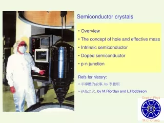
Dept of Phys M.C. Chang Semiconductor crystals • Overview • The concept of hole and effective mass • Intrinsic semiconductor • Doped semiconductor • p-n junction Refs for history: • 半導體的故事, by 李雅明 • 矽晶之火, by M.Riordan and L.Hoddeson
Elements Compounds Bonding becomes more ionic • (at 300K) Ge Si GaAs GaN • energy gap (eV) 0.67 (i) 1.11 (i) 1.43 (d) 3.39 (d) • lattice type Diamond Diamond Zincblend • Semiconductor is insulator at 0 K, but because of its smaller energy gap (diamond = 5.4 eV), electrons can be thermally excited to the conduction band more easily. • Si-based device can endure higher working temperature than Ge-based (75 oC) device (Si has a larger band gap) For history of semiconductor industry, see矽晶之火
Direct band gap (GaAs, GaN…) Indirect band gap (Si, Ge…) =Eg =Eg+ Direct band gap semiconductor can emit light efficiently (1μm=1.24 eV)
發明前 發明後 See Interview with Nakamura: Scientific American, July, 2000 The invention of blue-light LED GaN can emit blue light because of its large band gap (3.4 eV) • First blue-light LED: Shuji Nakamura 1989 • First blue-light laser: Shuji Nakamura 1997 中村秀二
Overview The concept of hole and effective mass Intrinsic semiconductor Doped semiconductor p-n junction
A nearly-filled band • ∴ unoccupied states behave as +e charge carriers A filled band does not carry current (Peierls, 1929) • Electric current density • For crystals with inversion symmetry, • n(k)= n(-k) • electrons with momenta ħk and -ħk have opposite velocities • no net current in equilibrium
The concept of holes (Peierls, 1929) If an electron of wavevector ke is missing, then k= -ke. Alternatively speaking, a hole with wavevector kh is produced (and kh= -ke). The lower in energy the missing electron lies, the higher the energy of the whole system. If the energy of a filled valence band is set to zero, then h k The missing electron
The concept of effective mass Near the bottom of a conduction band, the energy dispersion is approximately parabolic Reciprocal effective mass matrix The electron near band bottom is like a free electron (with m*). • For a spherical FS, m*ij=m*δij, one m* is enough. • In general, electron in a flatter band has a larger m* • Negative effective mass: • If E(k) is (e.g. top of valence band) then m*<0 • electron (-e) with negative m* = hole (+e) with positive m*
T L For ellipsoidal FS, there can be at most three different m*s Eg. the FS of Si is made of six identical ellipsoidal pockets • For Si, Eg = 1.1 eV, mL= 0.9 m, mT= 0.2 m (it’s more difficult for the electron to move along the L direction because the band is flatter along that direction)
More band structures and Fermi surfaces Common features Useful parameters mL /mT mHH/mLH Δ Si 0.91/0.19 0.46/0.16 0.044 eV GaAs 0.063 0.5/0.076 0.3 eV
Overview The concept of hole and effective mass Intrinsic semiconductor Doped semiconductor p-n junction
Density of states and carrier density • At room temperature, ε-μ >> kBT, electron density in conduction band: Top of valence band is set as E=0 • hole density in valence band:
Carrier density and energy gap Chemical potential In intrinsic semiconductor, • the density of intrinsic carriers depends only on the energy gap. The 2nd term is very small because kBT<<EG (For Si, the atom density is 5×1022cm-3.)
Impurity level: Bohr atom model • The ionized impurity atom has hydrogen-like potential, • (m m*, ε0 ε) • Dielectric constant of Si = 11.7 (Ge=15.8, GaAs=13.13) • Effective mass for Si =0.2 m • Therefore, the donor ionization energy = 20 meV. • Bohr radius of the donor electron, • For Si, it's about 50 A (justifies the use of a constant ε)
Impurity levels in Si Conduction band Valence band Energy-band point of view
The law of mass action When the doping density >> ni, we can simply ignore ni (for majority carrier). Then the density of minority carrier is determined by the law of mass-action.
Overview The concept of hole and effective mass Intrinsic semiconductor Doped semiconductor p-n junction (extra)
Equilibrium B.G. Streetman, Solid State Electronic Devices
Equilibrium With external bias Rectification B.G. Streetman, Solid State Electronic Devices