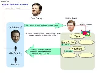
Delay Calculations
Delay Calculations. Section 6.1-6.4. Load Capacitance Calculation. C load = C self +C wire +C fanout. Fanout Capacitance. Fanout Gate Capacitance. C fanout : fanout capacitance due to the inputs of subsequent gates, C G . C fanout =C G1 +C G2 +C G3 ….

Delay Calculations
E N D
Presentation Transcript
Delay Calculations Section 6.1-6.4
Load Capacitance Calculation Cload=Cself+Cwire+Cfanout
Fanout Gate Capacitance • Cfanout: fanout capacitance due to the inputs of subsequent gates, CG. Cfanout=CG1+CG2+CG3…. Assumption: Each fanout is an inverter.
Input Capacitance Calculation • COL: overlap capacitance • CGN, CGP: Thin Oxide Capacitance
Worst Case Analysis Assumption • The thin-oxide capacitance is voltage dependent. • The worst case analysis uses CoxWL to compute its worst case value.
Thin Oxide Capacitance:Cg CG=WLCox=WL(εox/tox)=WCg Unit of Cg: fF/μm [Worst Case Analysis]
Cg Cg is approximately 1.61 fF/μm for the last 25 years. Exception: the 0.18 μm process, which has a Cg of 1.0 fF/ μm. [Worst Case Analysis]
Components of Col Col=Cf+Cov Cf:fringing capacitance Cov: overlap capacitance
Redefine Cg • For 0.13 μm, • Cg (due to tox alone): 1.6 fF/μm [Hodges, p.72] • Col(due to Cov and Cf): 0.25 fF/ μm [Hodges, p.80] • Redefine Cg [Hodges, p.259] as • Cg=CoxL+2Col • Cg =1.6 fF/μm+ 2 0.25 fF/μm=2 fF/μm • Cg has been constant for over 20 years • Multipy Cg by W to obtain the total capacitance due to tox, Cov and Cf [Worst Case Analysis] [Worst Case Analysis]
Gate Capacitance of an Inverter • CG=Cg(Wn+Wp) • CG=2fF/μm(Wn+Wp) [Worst Case Analysis]
Input Capacitance of a 3-input NAND Gate 2W 2W 2W 3W 3W 3W CG=Cg(Wn+Wp)=Cg(3W+2W)= Cg(5W)
Fanout Gate capacitance of n Inverters • Cfanout=2fF/μm[(Wn+Wp)1+(Wn+Wp)2…(Wn+Wp)n] For NANDs, NORs, apply the above equation with appropiate widths. [Worst Case Analysis]
Self-Capacitance Calculation Eliminate capacitors not connected to the output Assume the transistors are either on (Saturation) or off (Cutoff). CGD is negligible in either saturation or cutoff.
Calculation of Self-Capacitance of an Inverter Cself=CDBn+CDBP+2COL+2COL CDBn=CjnWn CDBp=CjpWp COL=ColW Cself=CjnWn+CjpWp+2Col(Wn+Wp) Assume Cjn=Cjp Cself=Ceff(Wn+Wp) For 0.13: Ceff=1 fF/μm [Hodges, p. 261]
Self-Capacitance of a NOR Condition: A=0 B=0→1 CDB4, CSB3 do not need to be charged.→NOT THE WORST CASE CDB3 is charged, while CDB1 and CDB2 are discharged. To avoid double counting, CDB1 and CDB2 will be called CDB12.
Self-Capacitance of NOR Constant Voltage at X
Self-Capacitance of a NOR WORST CASE!! CDB4 and CSB3 need to be charged CDB3 is charged, while CDB1 and CDB2 are discharged
Self-Capacitance of NOR WORST CASE!!
Wire Capacitance • Ignore wire capacitance if the length of a wire is less than a few microns. • Include wires longer than a few microns • Cwire=CintLwire • Cint=0.2 fF/um • For very long wires use distributed model
Example 6.4 • Capacitance Calculation for Inverter
Conclusion • Propagation delay depends on the arrival time of inputs • In a series stack, the delay increases as the late arriving input is further from the output.
Sequence: A: charges X B: charges Y C: discharges X, Y, CL Worst Case
Sequence: C: discharges X, (if any) B: discharges Y (if any) A: discharges CL Improved!
Design Strategy 1 • Reorder the inputs so that • the earliest signal arrive lower in the stack • The latest signals arrive near the top of the stack
Design Strategy 2 • To reduce delay: • WC>WB>WA • Problem: • Device capacitance are increased as the device sizes are increased.
Improve Delay Calculation with Input Slope iout=iNMOS-iPMOS Select Vin and Vout CalculateiNMOSandiPMOS Calculateiout
Simplified Inverter Output Current as a function of Vout and Vin
Example 6.5 • Compute the delay (tPHL,step) of a CMOS inverter due to a step input • Compute the delay (tPHL,step) of a CMOS inverter due to an input ramp with a rise time of tr
Conclusion from Example 6.5 tramp=Δtramp+tstep tstep=0.7RC Δtrampdepends on the trof the driving circuit. Δtramp=0.7RC/2=0.3RC Assumption: the tr is equal to 2tPLH