Download
1 / 41
430 likes | 638 Views
Calculate capacitances, delay, and sizing for CMOS inverter chains to optimize propagation delay. Analyze self-loading effect, device sizing, and load constraints affecting delay formula. Explore tapering and optimal stage sizing for minimum delay.

E N D
V DD PMOS Metal1 Polysilicon NMOS CMOS Inverters m m 0.25 =2l Out In GND
Device Sizing (for fixed load) Self-loading effect: Intrinsic capacitances dominate
NMOS/PMOS ratio tpHL tpLH tp b = Wp/Wn = 1.9
Inverter Chain In Out CL • If CL is given: • How many stages are needed to minimize the delay? • How to size the inverters? • May need some additional constraints.
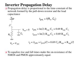
Inverter Delay • Minimum length/width devices, Lmin= Wmin = Wunit =0.25mm, • Assume that for WP = 2WN = 2W • same pull-up and pull-down currents • approx. equal resistances RN = RP • approx. equal rise tpLH and fall tpHL delays • Analyze as an RC network 2W W tpHL = (ln 2) RNCL Delay (D): tpLH = (ln 2) RPCL Load for the next stage:
Inverter with Load Delay RW CL RW Load (CL) tp = kRWCL k is a constant, equal to 0.69 Assumptions: no load -> zero delay
- - 1 1 æ ö æ ö W ç ÷ ç ÷ = = R R R S ç ÷ ç ÷ W unit unit W è ø è ø unit Inverter with Load CP = 2SCunit Delay WP = 2WN = 2W Cgin = CP + CN Cint = SCint_unit CL S = W / Wunit WN = W Load CN = SCunit Delay = kRW(Cint + CL) = kRWCint + kRWCL = kRW Cint(1+ CL /Cint) = Delay (Internal) + Delay (Load)
Delay Formula Cint = gCgin withg 1 f = CL/Cgin- effective fanout RW = Runit/S ; Cint =Scint_unit tp0 = 0.69RWCint = 0.69RunitCint_unit 0.69RunitCunit
Apply to Inverter Chain In Out CL 1 2 N tp = tp1 + tp2 + …+ tpN
Optimal Tapering for Given N • Delay equation has N - 1 unknowns, Cgin,2 – Cgin,N • Minimize the delay, find N - 1 partial derivatives • Result: Cgin,j+1/Cgin,j = Cgin,j/Cgin,j-1 • Size of each stage is the geometric mean of two neighbors • each stage has the same effective fanout (Cout/Cin) • each stage has the same delay
Optimum Delay and Number of Stages When each stage is sized by f and has same eff. fanout f: Effective fanout of each stage: Minimum path delay
Example In Out CL= 8 C1 1 f f2 C1 CL/C1 has to be evenly distributed across N = 3 stages:
Optimum Number of Stages For a given load, CL and given input capacitance Cin Find optimal sizing f For g = 0, f = e = 2.718, N = lnF
Optimum Effective Fanout f Optimum f for given process defined by g fopt = 3.6 forg=1
Impact of Self-Loading on tp No Self-Loading, g=0 With Self-Loading g=1
Buffer Design N f tp 1 64 65 2 8 18 3 4 15 4 2.8 15.3 1 64 1 8 64 1 4 64 16 1 64 22.6 8 2.8
D How to Design Large Transistors
Bonding Pad Design Bonding Pad GND 100 mm Out VDD Out In GND
Vdd Vin Vout C L Dynamic Power Dissipation 2 Energy/transition = C * V L dd 2 Power = Energy/transition * f = C * V * f L dd Not a function of transistor sizes! Need to reduce C , V , and f to reduce power. L dd
Adiabatic Charging 2 2 2
Transistor Sizing for Minimum Energy • Goal: Minimize Energy of whole circuit • Design parameters: f and VDD • tp tpref of circuit with f=1 and VDD =Vref VTE = VT + VDSAT/2
Transistor Sizing (2) • Performance Constraint (g=1) • Energy for single Transition
Transistor Sizing (3) VDD=f(f) E/Eref=f(f) F=1 2 5 10 20
How to keep Short-Circuit Currents Low? Short circuit current goes to zero if tfall at output >> trise at the input but can’t do this for cascade logic, so ...
Minimizing Short-Circuit Power Vdd =3.3 Vdd =2.5 Vdd =1.5
Leakage Sub-threshold current one of most compelling issues in low-energy circuit design!
Reverse-Biased Diode Leakage JS = 10-100 pA/mm2 at 25 deg C for 0.25mm CMOS JS doubles for every 9 deg C!
Static Power Consumption Wasted energy … Should be avoided in almost all cases, but could help reducing energy in others (e.g. sense amps)
Principles for Power Reduction • Prime choice: Reduce voltage! • Recent years have seen an acceleration in supply voltage reduction • Design at very low voltages still open question (0.6 … 0.9 V by 2010!) • Reduce switching activity • Reduce physical capacitance • Device Sizing: for F=20 • fopt(energy)=3.53, fopt(performance)=4.47