Download
1 / 29
290 likes | 437 Views
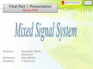
Final Part 1 Presentation Spring 2008. Mixed Signal System. Students: Alexander Kinko Roni Lavi Instructor: Inna Rivkin Duration: 2 Semesters. 3 Digital Experiments. 3 Analog Experiments. A/D – D/A. A little motivation …. Mixed Signal System (M.S.S.). Table of Contents.

E N D
Final Part 1 Presentation Spring 2008 Mixed Signal System Students: Alexander Kinko Roni Lavi Instructor: Inna Rivkin Duration: 2 Semesters
3 Digital Experiments 3 Analog Experiments A/D – D/A A little motivation … Mixed Signal System (M.S.S.)
Table of Contents • Main Goal • Project Overview • Project Implementation • Card Specifications • Accomplishments • VHDL Modules’ Description
Main Goal Giving the students in E.E. lab 1 a tool for a deeper understanding, designing and implementing of modern signal processing systems.
Project Overview (semester a) • Designing and manufacturing a new platform for real time M.S.S. experiment (Mixed Signal System), for audio signals. • Designing an analog application (audio circuit) that combines M.S.S. processing.
Project Overview (semester b) • Designing simple algorithms, that conduct signal processing in real time. • The platform will be incorporated in the future set of experiments in E.E. Lab 1, Technion.
Sample Real Time Digital Processing (DE2) Reconstruction Analog Input Analog Output Project Implementation (Top Level)
Matrix Analog Output Circuit (Smoothing Filter, Power amp) Analog Input (Mic/Sig. Gen.) Analog Outputs (Headphones/Scope) Analog Input Circuit (Anti-aliasing Filter, preamp) Oscillator (optional) Ext. Clock Analog Signal Analog Signals Reconstruction System (Multiplying DAC) ADDA Sampling System (ADC) Control Digital Interface User Control DE2 (Digital Processing) Project Implementation (Block Level)
Analog Outputs Analog Input DE2 Analog Input MATRIX User Control ADDA Project Implementation (Module Level) Digital Interface
Brief Description of AD7339 Main Features: ADC: Input voltage: ± 1V (biased internally around 1.4 V) Conversion Rate: 2.048 MSPS Parallel DACs: Output voltage: 2.5 ± 1.4 V Max. Update Rate: 2.304 MSPS Serial DACs: Output voltage: 0.2 V – 4.753 V
Card Specifications (Power Supply) • DC voltage supply: • Main DC power source from DE2: +5 V, +3.3 V • External DC power (optional): +9 V • DC current consumption: • +3.3 V: < 30mA • +5 V: ~ 150mA
Card Specifications (Inputs) • Analog input signal: • Bipolar voltage range: ±1 V • Input bandwidth: 20 Hz – 20 kHz • Protection from input over-voltage • External clock input (optional): • Voltage range: Standard LVTTL levels • Up to ~100 kHz
Card Specifications (Outputs) • 4 Analog output signals: • 4 channels with sample rate of 100 KSPS • Maximum update rate for 2 outputs of parallel DACs: 2.304 MSPS • Parallel DACs voltage range: ±1.4 V biased around 2.5 V • Serial DACs voltage range: 0.2 – 4.753 V • Ability to normalize all DAC outputs to ±1 V (dynamic range of A/D converter) around 2.5 V
Card Specifications (Control Inputs) The platform can function in several modes, that are controlledby mechanical switches located on the digital processing unit (DE2), featuring: • Mixed signal processing mode () • Self test mode (B.I.T. - Built In Test) () • Flexible clock source (internal or external)
Accomplishments • Designing and manufacturing A/D-D/A PCB card • Designing and building analog input stage • Full integration with DE2 • High and low level digital processing
DE2 CLK_50 BIT_Top (Application Level) ADDA CLK_50 ADC_Interface Buffers/ Voltage Level Translators Control Analog Input Internal 50 MHz DE2 Oscillator CLK_50 PDAC_Inteface CLK_50 CLK_50 CLK_50 SDAC_Interface CLK_Distributor Analog Outputs CLK_50 Control CLK_50 Seg_7_Interface Switch_Debouncer User Control 7-Segment Display Control VHDL Modules’Description (Top Level)
CLK_Distributor VHDL Modules’Description (Clock Distributor) ENTITY CLK_Distributor IS PORT ( CLK_IN : IN STD_LOGIC ; ENABLE_TO_ADC : OUT STD_LOGIC ; ENABLE_TO_PDAC_MODULE : OUT STD_LOGIC ; ENABLE_TO_SDAC_MODULE : OUT STD_LOGIC ; ENABLE_TO_DEBOUNCER_MODULE : OUT STD_LOGIC ; ENABLE_TO_BIT_MODE : OUT STD_LOGIC ; ENABLE_TO_BIT_MODE_RD_VALUES : OUT STD_LOGIC ); END CLK_Distributor;
VHDL Modules’Description (ADC Interface) ENTITY ADC_Interface IS PORT ( CLK_IN : IN STD_LOGIC ; RESETn : IN STD_LOGIC ; ENABLE : IN STD_LOGIC ; DATA_FROM_ADC : IN STD_LOGIC_VECTOR (7 DOWNTO 0) ; ADC_RESET : IN STD_LOGIC ; DATA_ENABLE_ADC : IN STD_LOGIC ; DATA_OUT : OUT STD_LOGIC_VECTOR (7 DOWNTO 0) ; CLK_TO_ADC : OUT STD_LOGIC ); END ADC_Interface;
VHDL Modules’Description (PDAC Interface) ENTITY PDAC_Interface IS PORT ( CLK_IN : IN STD_LOGIC ; RESETn : IN STD_LOGIC ; ENABLE : IN STD_LOGIC ; NORM_ENABLE : IN STD_LOGIC ; DATA_IN_PDAC_A : IN STD_LOGIC_VECTOR (7 DOWNTO 0) ; PDAC_A_RESET : IN STD_LOGIC ; DATA_IN_ENABLE_PDAC_A : IN STD_LOGIC ; DATA_TO_PDAC_A : OUT STD_LOGIC_VECTOR (7 DOWNTO 0) ; DATA_IN_PDAC_B : IN STD_LOGIC_VECTOR (7 DOWNTO 0) ; PDAC_B_RESET : IN STD_LOGIC ; DATA_IN_ENABLE_PDAC_B : IN STD_LOGIC ; DATA_TO_PDAC_B : OUT STD_LOGIC_VECTOR (7 DOWNTO 0) ; CLK_TO_PDACs : OUT STD_LOGIC ); END PDAC_Interface;
VHDL Modules’Description (SDAC Interface) ENTITY SDAC_Interface IS PORT ( CLK_IN : IN STD_LOGIC ; RESETn : IN STD_LOGIC ; ENABLE : IN STD_LOGIC ; SCAN_ENABLE : IN STD_LOGIC ; NORM_ENABLE : IN STD_LOGIC ; DATA_IN_SDAC0 : IN STD_LOGIC_VECTOR(7 DOWNTO 0) ; SDAC0_RESET : IN STD_LOGIC ; DATA_IN_SDAC0_ENABLE : IN STD_LOGIC ; DATA_IN_SDAC1 : IN STD_LOGIC_VECTOR(7 DOWNTO 0) ; SDAC1_RESET : IN STD_LOGIC ; DATA_IN_SDAC1_ENABLE : IN STD_LOGIC ; SDATA_OUT : OUT STD_LOGIC ; SCLK_OUT : OUT STD_LOGIC ; SLATCH_OUT : OUT STD_LOGIC ); END SDAC_Interface;
VHDL Modules’Description (7 Segment Interface) ENTITY Seg_7_Interface IS PORT ( CLK_IN : IN STD_LOGIC ; RESETn : IN STD_LOGIC ; ENABLE : IN STD_LOGIC ; HEX7_IN : IN STD_LOGIC_VECTOR(4 DOWNTO 0) ; HEX7_ENABLE : IN STD_LOGIC ; HEX6_IN : IN STD_LOGIC_VECTOR(4 DOWNTO 0) ; HEX6_ENABLE : IN STD_LOGIC ; HEX5_IN : IN STD_LOGIC_VECTOR(4 DOWNTO 0) ; HEX5_ENABLE : IN STD_LOGIC ; HEX4_IN : IN STD_LOGIC_VECTOR(4 DOWNTO 0) ; HEX4_ENABLE : IN STD_LOGIC ; HEX3_IN : IN STD_LOGIC_VECTOR(4 DOWNTO 0) ; HEX3_ENABLE : IN STD_LOGIC ; HEX2_IN : IN STD_LOGIC_VECTOR(4 DOWNTO 0) ; HEX2_ENABLE : IN STD_LOGIC ; HEX1_IN : IN STD_LOGIC_VECTOR(4 DOWNTO 0) ; HEX1_ENABLE : IN STD_LOGIC ; HEX0_IN : IN STD_LOGIC_VECTOR(4 DOWNTO 0) ; HEX0_ENABLE : IN STD_LOGIC ; HEX7 : OUT STD_LOGIC_VECTOR (6 DOWNTO 0); HEX6 : OUT STD_LOGIC_VECTOR (6 DOWNTO 0); HEX5 : OUT STD_LOGIC_VECTOR (6 DOWNTO 0); HEX4 : OUT STD_LOGIC_VECTOR (6 DOWNTO 0); HEX3 : OUT STD_LOGIC_VECTOR (6 DOWNTO 0); HEX2 : OUT STD_LOGIC_VECTOR (6 DOWNTO 0); HEX1 : OUT STD_LOGIC_VECTOR (6 DOWNTO 0); HEX0 : OUT STD_LOGIC_VECTOR (6 DOWNTO 0) ); END Seg_7_Interface;
VHDL Modules’Description (Switch Debouncer) ENTITY Switch_Debouncer IS PORT ( CLK_IN : IN STD_LOGIC ; RESETn : IN STD_LOGIC ; ENABLE : IN STD_LOGIC ; SW : IN STD_LOGIC_VECTOR(17 DOWNTO 0) ; SW_DEB : OUT STD_LOGIC_VECTOR(17 DOWNTO 0) ); END Switch_Debouncer;
Where Are We Standing ? • Manufacturing PCB Done • 2 assembled circuits We have 12 (assembled & checked) out of 24 manufactured PCBs • Basic M.S.S. system Done • Basic DSP functions Done
What’s else to come …? • Finish to assemble and check rest of PCBs • To plan an experiment setup (with Amos & Jan) • Enriching simple DSP algorithms • Publish a user manual of the project • Publish an experiment brief
Special Thanks to: Inna Rivkin Supervisor Eli Shoshan Mentor and support Ella Glozman For her dedicated work Bruria Zohar For all the help and supplies The Entire HS-DSL Staff
DE2 + ADDA Headphones Scope MIC. Pre-AMP MIC Bank of 4 LPFs One Picture Is Worth A Thousand Words …