Download

1 / 18
200 likes | 436 Views
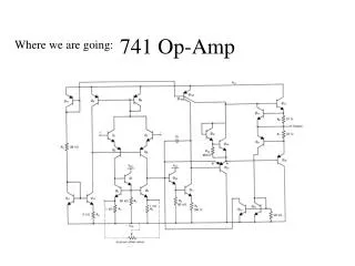
Nonideal Op Amp Characteristics. Presenter : 蔡錦成 Advisor : Dr. Chih-Kuo Liang Date: 2007/1/10. Outline. Nonideal DC Characteristics. Data Sheet. Input Bias Current Effect (1/4). FET<<BJT. V+. Rc1. Rc2. 輸入偏壓電流 ( Input Bias Current ). ( + ). Q1. Q2. ( - ). 典型值 100 nA. Re2. Re1.

E N D
Nonideal Op Amp Characteristics Presenter :蔡錦成 Advisor : Dr. Chih-Kuo Liang Date: 2007/1/10
Outline • Nonideal DC Characteristics
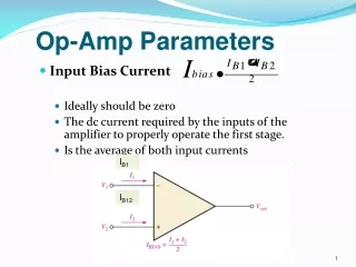
Input Bias Current Effect (1/4) FET<<BJT V+ Rc1 Rc2 輸入偏壓電流 (Input Bias Current) ( + ) Q1 Q2 ( - ) 典型值100 nA Re2 Re1 輸入直流抵補電流 (Input DC Offset Current) V- 典型值10 nA BJT偏壓電流
Input Bias Current Effect (2/4) Ideal Reality - - Vo=0 Vo≠0 + + Vo=Voso (Output DC Offset Voltage) - Vosi Voso=Aol .Vosi + Equivalent circuit 輸入直流抵補電壓 Vosi
Vosi Vs Input Bias Current Effect (3/4) Example - Vo + Ideal Reality
Input Bias Current Effect (4/4) - Vo + (只有考慮偏壓電流) 當Vs=0 Vo≠0 (考慮偏壓電流+ Vosi ) 當Vs=0 Vo≠0
Better Input Bias Current 理想運算放大器 - 非理想運算放大器 ro Vo + 改善偏壓電流
ro Vo 利用重疊定理求出Vo (1/2) (a) + - (b)
120 K 27 K Vo 741 68 K Example 已知 : 求 Vo ? Ans :
120 K 27 K Vo 741 Minimize effect (1/3)
120 K 27 K Vo 741 Minimize effect (2/3)
Minimize effect (3/3) 120 K 27 K Vo 741 22 K
DC Offset Way 1. 內部補償方法 Vcc - Vo + - Vo + (歸零調整) (修正調整) Vcc or -Vcc R2 R1 Vcc - 2. 外部補償方法 Vo + Vs -Vcc Vcc Vp R4 R3 R1//R2 -Vcc
Drift Temperature drift Input offset current Input offset voltage Temperature change 減少漂移現象
V1 Ro Vo Output Resistance <<1