Download

1 / 78
780 likes | 803 Views
Learn about the electrical characteristics of an ideal operational amplifier, including input specifications, bias current, offset voltage, power supply rejection ratio, and noise. Understand how to calculate and interpret voltage and current noise in an op amp circuit.

E N D
Deciphering Electrical Characteristics in an Op Amp Datasheet Tim Green Linear Applications Manager Tucson Division green_tim@ti.com
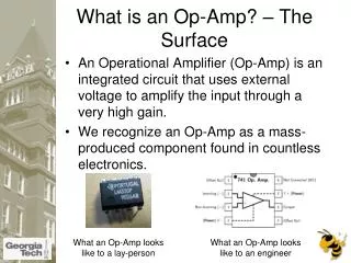
Ideal Operational Amplifier • Zero input current • Infinite input resistance • Infinite open loop gain • Zero output resistance • Infinite Slew Rate
Ideal Operational Amplifier VOUT = (VINP – VINM) * Aol VOUT / Aol – VINP = -VINM If Aol = ∞ (for an Ideal Op Amp) then: -VINP = -VINM or VINP = VINM
Input Specifications • Input Bias Current (Ib) & Input Offset Current (Ios) • Input Offset Voltage (Vos) • Power Supply Rejection Ratio (PSRR): Referred-To-Input Vos • Common Mode Voltage Range (Vcm) • Common Mode Rejection Ratio (CMRR): Referred-To-Input Vos • Small Signal Input Parasitics: Input Capacitance, Input Resistance • Input Noise: Current, Voltage (in, en)
Input Bias Current (Ib), Input Offset Current (Ios) Ib = 5pA Ios = 4pA Polarity is + or – Current into or out of inputs
Input Bias Current (Ib), Input Offset Current (Ios) 25C Specs in Table Often Curves for Temperature Specs Polarity is + or –
Input Offset Voltage (Vos) Vout Error 25C Specs in Table Often Histograms show distribution of Vos Polarity is + or –
Input Offset Voltage (Vos) Drift Vout Error Vos Drift Specs in Table Often Histograms show distribution of Vos Drift Polarity is + or -
Power Supply Rejection Ratio (PSRR) Vout Error DC PSRR in Table DC PSRR Drift in Table Polarity is + or - PSRR is an RTI (Referred-To-Input) specification Appears as Input Offset Voltage
Power Supply Rejection Ratio (PSRR) Vout Error 20kHz AC PSRR in Curve PSRR is an RTI (Referred-To-Input) specification Appears as Input Offset Voltage
Common Mode Voltage Range (Vcm) Vcm Same for DC & AC AC peak voltage < Vcm
Common Mode Rejection Ratio (CMRR) Vout Error CMRR DC in Table Polarity is + or - CMRR is an RTI (Referred-To-Input) specification Appears as Input Offset Voltage
Common Mode Rejection Ratio (CMRR) Vout Error AC CMRR in Curve CMRR is an RTI (Referred-To-Input) specification Appears as Input Offset Voltage
Small SignalInput Parasitics Rdiff > 200GW for Bipolar Inputs Rcm > 40MW for Bipolar Inputs Even greater for JFET or MOSFET inputs Ccm, Cdiff in Table Rcm, Rdiff in Table if specified Ccm and Cdiff can be a problem: Ccm and Cdiff form Cin Cin & RF form a Loop Gain pole unwanted oscillations depending upon UGBW and value of RF.
Op Amp Noise Model VN IN+ IN- Noise Model (IN+ and IN- are not correlated) OPA277 Data Tina Simplified Model VN IN
Understanding The Spectrum:Total Noise Equation (Current or Voltage) enT = √[(en1/f)2 + (enBB)2] where: enT = Total rms Voltage Noise in volts rms en1/f = 1/f voltage noise in volts rms enBB = Broadband voltage noise in volts rms
Real Filter Correction vs Brickwall Filter where: fP = roll-off frequency of pole or poles fBF = equivalent brickwall filter frequency
AC Noise Bandwidth Ratios for nth Order Low-Pass Filters BWn = (fH)(Kn) Effective Noise Bandwidth Real Filter Correction vs Brickwall Filter
eBB Broadband Noise Equation BWn = (fH)(Kn) where: BWn = noise bandwidth for a given system fH = upper frequency of frequency range of operation Kn = “Brickwall” filter multiplier to include the “skirt” effects of a low pass filter enBB = (eBB)(√[BWn]) where: enBB = Broadband voltage noise in volts rms eBB = Broadband voltage noise density ; usually in nV/√Hz BWn = Noise bandwidth for a given system
en1/f = (e1/f@1Hz)(√[ln(fH/fL)]) where: en1/f = 1/f voltage noise in volts rms over frequency range of operation e1/f@1Hz = voltage noise density at 1Hz; (usually in nV) fH = upper frequency of frequency range of operation (Use BWn as an approximation for fH) fL = lower frequency of frequency range of operation e1/f@1Hz = (e1/f@f)(√[f]) where: e1/f@1Hz = normalized noise at 1Hz (usually in nV) e1/f@f = voltage noise density at f ; (usually in nV/√Hz) f = a frequency in the 1/f region where noise voltage density is known e1/f@1Hz 1/f Noise Equation
Example Noise Calculation Given: OPA627 Noise Gain of 101 Find (RTI, RTO): Voltage Noise Current Noise Resistor Noise
Voltage Noise Spectrum and Noise Bandwidth 50nV/rt-Hz 5nV/rt-Hz Unity Gain Bandwidth = 16MHz Closed Loop Bandwidth = 16MHz / 101 = 158kHz
Example Voltage Noise Calculation Voltage Noise Calculation: Broadband Voltage Noise Component: BWn ≈ (fH)(Kn) (note Kn = 1.57 for single pole) BWn ≈ (158kHz)(1.57) =248kHz enBB = (eBB)(√BWn) enBB = (5nV/√Hz)(√248kHz) = 2490nV rms 1/f Voltage Noise Component: e1/f@1Hz = (e1/f@f)(√f) e1/f@1Hz = (50nV/√Hz)(√1Hz) = 50nV en1/f = (e1/f@1Hz)(√[ln(fH/fL)]) Use fH = BWn en1/f = (50nV)(√[ln(248kHz/1Hz)]) = 176nV rms Total Voltage Noise (referred to the input of the amplifier): enT = √[(en1/f)2 + (enBB)2] enT = √[(176nV rms)2 + (2490nV rms)2] = 2496nV rms
Example Current Noise Calculation Note: This example amp doesn’t have 1/f component for current noise. en-in= (in)x(Req) en-out= Gain x (in)x(Req)
Example Current Noise Calculation Broadband Current Noise Component: BWn ≈ (fH)(Kn) BWn ≈ (158kHz)(1.57) =248kHz inBB = (iBB)(√BWn) inBB = (2.5fA/√Hz)(√248kHz) = 1.244pA rms Req = Rf || R1 = 100k || 1k = 0.99k eni = (In)( Req) = (1.244pA)(0.99k) = 1.23nV rms Since the Total Voltage noise is envt = 2496nV rms the current noise can be neglected. neglect
Resistor Noise – Thermal Noise The mean- square open- circuit voltage (e) across a resistor (R) is: en = √ (4kTKRΔf) where: TK is Temperature (ºK) R is Resistance (Ω) f is frequency (Hz) k is Boltzmann’s constant (1.381E-23 joule/ºK) en is volts (VRMS) To convert Temperature Kelvin to TK = 273.15oC + TC
Resistor Noise – Thermal Noise Noise Spectral Density vs. Resistance en density = √ (4kTKR) Noise Spectral Density vs. Resistance nV/rt-Hz Resistance (Ohms)
Example Resistor Noise Calculation enr = √(4kTKRΔf) where: R = Req = R1||Rf Δf = BWn enr = √(4 (1.38E-23)(273 + 25) (0.99k)(248kHz)) = 2010nV rms en-in= √(4kTRΔf) en-out= Gain x (√(4kTRΔf))
Total Noise Calculation Voltage Noise From Op-AmpRTI: env = 2510nV rms Current Noise From Op-Amp RTI (as a voltage): eni = 1.24nV rms Resistor Noise RTI: enr = 2020nV rms Total Noise RTI: en in = √((2510nV)2 + ((1.2nV)2 + ((2010nV)2) = 3216nV rms Total Noise RTO: en out = en in x gain = (3216nV)(101) = 325uV rms
Calculating Noise Vpp from Noise Vrms Relation of Peak-to-Peak Value of AC Noise Voltage to rms Value *Common Practice is to use: Peak-to-Peak Amplitude= 6 X rms
Voltage Noise (f = 0.1Hz to 10Hz) Low Frequency Low frequency noise spec and curve: Over specific frequency range: 0.1Hz < f < 10Hz Given as Noise Voltage in pp units Measured After Bandpass Filter: 0.1Hz Second−Order High−Pass 10Hz Fourth−Order Low−Pass
Frequency Response Specifications • Open Loop Gain (Aol) & Phase • Slew Rate (SR) • Total Harmonic Distortion + Noise (THD+N) • Settling Time (ts)
Open Loop Gain & Phase Open-Loop Voltage Gain at DC Linear operation conditions NOT the same as Voltage Output Swing to Rail Gain-Bandwidth Product = UGBW (Unity Gain Bandwidth) G=1 Stable Op Amps 5.5MHz
Vout/Vin:Gain Accuracy & Frequency Response fcl 1/Beta Vout/Vin
Slew Rate Slew Rate Measurement: 10% to 90% of Vout
Slew Rate &Full Power BandwidthorMaximum Output Voltage vs Frequency
THD + Noise Larger Closed Loop Gain Loop Gain to correct for Op Amp Non-Linearities and Noise
THD + Noise = 1% Example Fundamental f = Input Frequency Fundamental f = 99% Vout Amplitude Harmonics due to Op Amp non-linearities Noise due to Op Amp Input Noise (en, in) Harmonics + Noise < 1% of Vout
Settling Time Slew Rate Note: Settling Time includes Slew Rate time
Settling Time Settling Time Large Signal effects: Slew Rate Small Signal effects Large Gain = Less closed loop Bandwidth Large Gain = Less Loop Gain (AolB) to correct for errors Large Gain = Longer Settling Time
Output Specifications • Voltage Output Swing from Rail • Short Circuit Current (Isc) • Open Loop Output Impedance (Zo) • Closed Loop Output Impedance (Zout) • Capacitive Load Drive
Voltage Output Swing From Rail Loaded Vout swing from Rail Higher Current Load Farther from Rail Higher Current Load Larger Vsat Vsat = Vs - Vout +25C Curve: Op Amp Aol is degraded if on curve Op Amp Aol is okay if left of curve 1 2 1 2
Short Circuit Current (Isc) Output shorted Current Limit engaged For Graph shown TJ max is okay If using larger voltages (i.e. +5V, Gnd) use Short-Circuit Current values & analyze power dissipation and TJ max