Download

1 / 39
390 likes | 582 Views
NSNI – 2010, Mumbai, India. Development of high speed waveform sampling ASICs. Stefan Ritt - Paul Scherrer Institute, Switzerland. Question …. 4 channels 5 GSPS 1 GHz BW 8 bit (6-7) 15k$ (700kRs). 4 channels 5 GSPS 1 GHz BW 11.5 bits 1k$ (50kRs) USB Power.

E N D
NSNI – 2010, Mumbai, India Development of high speed waveform sampling ASICs Stefan Ritt - Paul Scherrer Institute, Switzerland
Question … 4 channels 5 GSPS 1 GHz BW 8 bit (6-7) 15k$ (700kRs) 4 channels 5 GSPS 1 GHz BW 11.5 bits 1k$ (50kRs) USB Power NSNI-2010 Mumbai
Switched Capacitor Array 0.2-2 ns Inverter “Domino” ring chain IN Waveform stored Out FADC 33 MHz Clock Shift Register “Time stretcher” GHz MHz NSNI-2010 Mumbai
Switched Capacitor Array • Cons • No continuous acquisition • Limited sampling depth • Nonlinear timing • Pros • High speed (up to 5 GSPS) high resolution (13 bit SNR) • High channel density (16 channels on 5x5 mm2) • Low power (10-40 mW / channel) • Low cost (~ 10$ / channel) Dt Dt Dt Dt Dt Goal: Minimize Limitations NSNI-2010 Mumbai
Design Options • CMOS process (typically 0.35 … 0.13 mm) sampling speed • Number of channels, sampling depth, differential input • PLL for frequency stabilization • Input buffer or passive input • Analog output or (Wilkinson) ADC • Internal trigger PLL Trigger ADC NSNI-2010 Mumbai
Write Circuitry How to sample the input signal
0 0 0 0 0 0 1 0 0 0 0 0 0 0 0 0 0 0 0 0 0 0 1 0 0 1 0 0 0 0 0 0 0 0 0 0 0 0 0 0 0 0 0 0 1 0 0 0 Simple inverter chain 0 0 0 0 0 0 1 0 0 0 0 0 0 0 0 0 0 0 1 1 1 1 1 0 0 1 1 1 1 1 1 1 1 1 1 1 1 1 1 1 1 1 0 0 0 1 1 1 NSNI-2010 Mumbai
Design of Inverter Chain PMOS > NMOS PMOS < NMOS NSNI-2010 Mumbai
“Tail Biting” speed enable 1 2 3 4 1 2 3 4 NSNI-2010 Mumbai
Phase Locked Loop • On-chip PLL can lock sampling frequency to external reference clock Inverter Chain sampling speed control PLL F1 T Q Phase Comparator up loop filter down External Reference Clock F2 NSNI-2010 Mumbai
Timing jitter • Inverter chain has transistor variations Dti between samples differ “Fixed pattern aperture jitter” • “Differential temporal nonlinearity” TDi= Dti – Dtnominal • “Integral temporal nonlinearity”TIi = SDti – iDtnominal • “Random aperture jitter” = variation of Dti between measurements Dt1 Dt2 Dt3 Dt4 Dt5 TD1 TI5 NSNI-2010 Mumbai
Fixed jitter calibration • Fixed jitter is constant over time, can be measured and corrected for • Several methods are commonly used • Most use sine wave with random phase and correct for TDi on a statistical basis NSNI-2010 Mumbai
Fixed Pattern Jitter Results • TDi typically ~50 ps RMS @ 5 GHz • TIi goes up to ~600 ps • Jitter is mostly constant over time, measured and corrected • Residual random jitter 3-4 ps RMS NSNI-2010 Mumbai
Achievable Timing Resolution • After proper timing calibration, a “split pulse timing accuracy” of typically~10 ps can be chieved D. BretonPicosecond Workshop Clermont-Ferrand, Jan 2010 NSNI-2010 Mumbai
What determines the BW? • The analog bandwidth is given by the parasitic capacitance of the input bus and the input impedance • Typically 20fF/cell+20pF (bus), 2-3 W for bond wire 1 GHz BW • An active input buffer does not really help Bond wire 2-3 W 20 pF 20 fF “The best buffer is no buffer” – G. Varner NSNI-2010 Mumbai
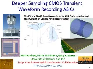
input shift register . . . . . . . . . . . . . . . . . . . . . . . . . . . . . . . . . secondary sampling stage fast sampling stage Cascaded Switched Capacitor Array • Combines the advantage of a short input stage (32 cells) with a deep secondary sampling stage (32x32 cells) • Estimated input BW:5 GHz • Sampling speed:10 GSPS (130 nm) • 100 ps sample time –3.1 ns hold time • Matches BW of fastestdetectors (G-APD, MCP-PMT) • next generation of SCAs NSNI-2010 Mumbai
Readout Circuitry How to read out sampled waveforms
Analog Readout Methods Uin “Differential Pair” write read Uin read Vout C (200fF) write R (700 ) C I ~ kT Ib/2 Ib/2 I Uin Ib read write + - . . . C NSNI-2010 Mumbai
Digital Readout • Wilkinson-type ADC requires only one comparator per sampling cell ramp voltage + comparator + comparator - - ASIC 12-bit counter latch latch DAC FPGA NSNI-2010 Mumbai
How to minimize dead time ? • Fast analog readout: 30 ns / sample • Parallel readout • Region-of-interestreadout • Simultaneouswrite / read DRS4 AD9222 12 bit 8 channels NSNI-2010 Mumbai
DRS4 ROI readout mode delayed trigger stop normal trigger stop after latency stop Trigger Delay 33 MHz e.g. 100 samples @ 33 MHz 3 us dead time 300,000 events / sec. readout shift register Patent pending! NSNI-2010 Mumbai
readout Channel 0 1 Channel 0 1 0 1 Channel 1 Channel 1 Channel 2 Simultaneous Write/Read FPGA 0 Channel 0 0 Channel 1 8-foldanalog multi-eventbuffer Channel 2 0 Channel 3 0 Channel 4 0 Channel 5 0 Channel 6 0 Channel 7 0 Expected crosstalk ~few mV NSNI-2010 Mumbai
Current SCA ASICs [1] E. Delagnes, D. Breton et al., NIM A567 (2006) 21 [2] G. Varner et al., NIM A583 (2007) 447 [3] S. Ritt, NIM A518 (2004) and http://drs.web.psi.ch [4] M. Sukhwani et al., NSNI 2010 NSNI-2010 Mumbai
Advanced Topics Triggering, Channel Cascading, Waveform Analysis
How to measure best timing? Simulation of MCP with realistic noise and different discriminators J.-F. Genat et al., arXiv:0810.5590 (2008) NSNI-2010 Mumbai
Baseline Restoration Transimpedance Preamplifier PMT/APD Wire FADC “Fast”12 bit Digital Processing Flash ADC Technique FADC Q-sensitive Preamplifier 60 MHz12 bit Shaper PMT/APD Wire Amplitude TDC Time • Shaper is used to optimize signals for “slow” 60 MHz FADC • Shaping stage can only remove information from the signal • Shaping is unnecessary if FADC is “fast” enough • All operations (CFD, optimal filtering, integration) can be done digitally NSNI-2010 Mumbai
How fast is “fast” • Nyquist-Shannon: Sampling rate must be 2x the highest frequency coming from detector • Analog Bandwidth must match signal from detector • Fastest pulses coming from Micro-Channel-Plate PMTs 3mm pores NSNI-2010 Mumbai
input shift register Aimed parameters: 5 GHz Bandwidth 10 GSPS Sampling Rate . . . . . . . . . . . . . . . . . . . . . . . . . . . . . . . . . 10 GSPS 30 GSPS secondary sampling stage fast sampling stage Fastest pulses • MCP-PMTs: 70 ps rise time 4-5 GHz BW 10 GSPS • Cable should not limit bandwidth Put digitizer onto detector • Higher sampling speed only improves statistics J. Milnes, J. Howoth, Photek NSNI-2010 Mumbai
DRS4 MUX Trigger and DAQ on same board • All SCA applications need some kind of trigger split signals • Using a multiplexer in DRS4, input signals can simultaneously digitized at 65 MHz and sampled in the DRS • FPGA can make local trigger(or global one) and stop DRSupon a trigger • DRS readout (5 GSPS)though same 8-channel FADCs global trigger bus trigger FPGA DRS FADC12 bit 65 MHz analog front end LVDS SRAM “Free” local trigger capability without additional hardware NSNI-2010 Mumbai
Daisy-chaining of channels Domino Wave Domino Wave clock clock enable input enable input 1 Channel 0 0 Channel 0 enable input enable input 0 Channel 1 1 Channel 1 Channel 2 0 Channel 2 1 Channel 3 Channel 3 1 0 Channel 4 Channel 4 0 1 Channel 5 Channel 5 1 0 Channel 6 Channel 6 0 1 Channel 7 Channel 7 1 0 DRS4 can be partitioned in: 8x1024, 4x2048, 2x4096, 1x8192 cellsChip daisy-chaining possible to reach virtually unlimited sampling depth NSNI-2010 Mumbai
G. Varner et al., Nucl.Instrum.Meth. A583, 447 (2007) Interleaved sampling 6 GSPS * 8 = 48 GSPS delays (167ps/8 = 21ps) Possible if delay is implemented on PCB NSNI-2010 Mumbai
On-line waveform display S848 PMTs “virtual oscilloscope” template fit click pedestal histo NSNI-2010 Mumbai
Pulse shape discrimination Example: a/g source in liquid xenon detector (or: g/p in air shower) a g Leading edge Decay time AC-coupling Reflections NSNI-2010 Mumbai
t-distribution ta = 21 ns tg = 34 ns Waveforms can be clearly distinguished a g NSNI-2010 Mumbai
Template Fit • Determine “standard” PMT pulse by averaging over many events “Template” • Find hit in waveform • Shift (“TDC”) and scale (“ADC”)template to hit • Minimize c2 • Compare fit with waveform • Repeat if above threshold • Store ADC & TDC values pb Experiment 500 MHz sampling Pile-up can be detected if two hits are separated in time by ~rise time of signal NSNI-2010 Mumbai
G. Varner Belle-TOF cPCI GBit Ethernet H. Friedrich WaveDREAM PSI/ETHZ Do we still need crates? • An empty crate slot costs ~1k$ (crate, interface/computer, cooling) • Crate topologies requires long cables Reduction of bandwidth • Alternative: Put electronics on detectors MEG 3000 channels NSNI-2010 Mumbai
Experiments using SCA ASCIs MEG 3000 channels MAGIC-II H.E.S.S. ANITA ANTARES Belle-TOF NSNI-2010 Mumbai
Conclusions • Fast waveform digitizing with SCA chips will have a big impact on experiments in the next future, replacing traditional ADCs and TDCs • SCA community growing! Exchange ofexperience is important. Joining is easy(e.g. USB evaluation boards) • New generation of SCA chips on the horizon NSNI-2010 Mumbai
Thank You! NSNI-2010 Mumbai