Download

1 / 39
390 likes | 419 Views
Development of high-speed waveform sampling ASICs for data acquisition systems. The ASICs offer fast sampling rates, high resolution, and low power consumption. Explore the design options, circuitry, jitter calibration, achievable timing resolution, readout methods, and minimizing dead time. Learn about advanced topics such as triggering, channel cascading, and waveform analysis.

E N D
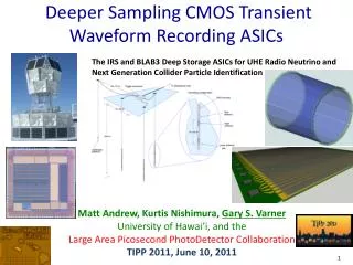
NSNI – 2010, Mumbai, India Development of high speed waveform sampling ASICs Stefan Ritt - Paul Scherrer Institute, Switzerland
Question … 4 channels 5 GSPS 1 GHz BW 8 bit (6-7) 15k$ (700kRs) 4 channels 5 GSPS 1 GHz BW 11.5 bits 1k$ (50kRs) USB Power NSNI-2010 Mumbai
Switched Capacitor Array 0.2-2 ns Inverter “Domino” ring chain IN Waveform stored Out FADC 33 MHz Clock Shift Register “Time stretcher” GHz MHz NSNI-2010 Mumbai
Switched Capacitor Array • Cons • No continuous acquisition • Limited sampling depth • Nonlinear timing • Pros • High speed (up to 5 GSPS) high resolution (13 bit SNR) • High channel density (16 channels on 5x5 mm2) • Low power (10-40 mW / channel) • Low cost (~ 10$ / channel) Dt Dt Dt Dt Dt Goal: Minimize Limitations NSNI-2010 Mumbai
Design Options • CMOS process (typically 0.35 … 0.13 mm) sampling speed • Number of channels, sampling depth, differential input • PLL for frequency stabilization • Input buffer or passive input • Analog output or (Wilkinson) ADC • Internal trigger PLL Trigger ADC NSNI-2010 Mumbai
Write Circuitry How to sample the input signal
0 0 0 0 0 0 1 0 0 0 0 0 0 0 0 0 0 0 0 0 0 0 1 0 0 1 0 0 0 0 0 0 0 0 0 0 0 0 0 0 0 0 0 0 1 0 0 0 Simple inverter chain 0 0 0 0 0 0 1 0 0 0 0 0 0 0 0 0 0 0 1 1 1 1 1 0 0 1 1 1 1 1 1 1 1 1 1 1 1 1 1 1 1 1 0 0 0 1 1 1 NSNI-2010 Mumbai
Design of Inverter Chain PMOS > NMOS PMOS < NMOS NSNI-2010 Mumbai
“Tail Biting” speed enable 1 2 3 4 1 2 3 4 NSNI-2010 Mumbai
Phase Locked Loop • On-chip PLL can lock sampling frequency to external reference clock Inverter Chain sampling speed control PLL F1 T Q Phase Comparator up loop filter down External Reference Clock F2 NSNI-2010 Mumbai
Timing jitter • Inverter chain has transistor variations Dti between samples differ “Fixed pattern aperture jitter” • “Differential temporal nonlinearity” TDi= Dti – Dtnominal • “Integral temporal nonlinearity”TIi = SDti – iDtnominal • “Random aperture jitter” = variation of Dti between measurements Dt1 Dt2 Dt3 Dt4 Dt5 TD1 TI5 NSNI-2010 Mumbai
Fixed jitter calibration • Fixed jitter is constant over time, can be measured and corrected for • Several methods are commonly used • Most use sine wave with random phase and correct for TDi on a statistical basis NSNI-2010 Mumbai
Fixed Pattern Jitter Results • TDi typically ~50 ps RMS @ 5 GHz • TIi goes up to ~600 ps • Jitter is mostly constant over time, measured and corrected • Residual random jitter 3-4 ps RMS NSNI-2010 Mumbai
Achievable Timing Resolution • After proper timing calibration, a “split pulse timing accuracy” of typically~10 ps can be chieved D. BretonPicosecond Workshop Clermont-Ferrand, Jan 2010 NSNI-2010 Mumbai
What determines the BW? • The analog bandwidth is given by the parasitic capacitance of the input bus and the input impedance • Typically 20fF/cell+20pF (bus), 2-3 W for bond wire 1 GHz BW • An active input buffer does not really help Bond wire 2-3 W 20 pF 20 fF “The best buffer is no buffer” – G. Varner NSNI-2010 Mumbai
input shift register . . . . . . . . . . . . . . . . . . . . . . . . . . . . . . . . . secondary sampling stage fast sampling stage Cascaded Switched Capacitor Array • Combines the advantage of a short input stage (32 cells) with a deep secondary sampling stage (32x32 cells) • Estimated input BW:5 GHz • Sampling speed:10 GSPS (130 nm) • 100 ps sample time –3.1 ns hold time • Matches BW of fastestdetectors (G-APD, MCP-PMT) • next generation of SCAs NSNI-2010 Mumbai
Readout Circuitry How to read out sampled waveforms
Analog Readout Methods Uin “Differential Pair” write read Uin read Vout C (200fF) write R (700 ) C I ~ kT Ib/2 Ib/2 I Uin Ib read write + - . . . C NSNI-2010 Mumbai
Digital Readout • Wilkinson-type ADC requires only one comparator per sampling cell ramp voltage + comparator + comparator - - ASIC 12-bit counter latch latch DAC FPGA NSNI-2010 Mumbai
How to minimize dead time ? • Fast analog readout: 30 ns / sample • Parallel readout • Region-of-interestreadout • Simultaneouswrite / read DRS4 AD9222 12 bit 8 channels NSNI-2010 Mumbai
DRS4 ROI readout mode delayed trigger stop normal trigger stop after latency stop Trigger Delay 33 MHz e.g. 100 samples @ 33 MHz 3 us dead time 300,000 events / sec. readout shift register Patent pending! NSNI-2010 Mumbai
readout Channel 0 1 Channel 0 1 0 1 Channel 1 Channel 1 Channel 2 Simultaneous Write/Read FPGA 0 Channel 0 0 Channel 1 8-foldanalog multi-eventbuffer Channel 2 0 Channel 3 0 Channel 4 0 Channel 5 0 Channel 6 0 Channel 7 0 Expected crosstalk ~few mV NSNI-2010 Mumbai
Current SCA ASICs [1] E. Delagnes, D. Breton et al., NIM A567 (2006) 21 [2] G. Varner et al., NIM A583 (2007) 447 [3] S. Ritt, NIM A518 (2004) and http://drs.web.psi.ch [4] M. Sukhwani et al., NSNI 2010 NSNI-2010 Mumbai
Advanced Topics Triggering, Channel Cascading, Waveform Analysis
How to measure best timing? Simulation of MCP with realistic noise and different discriminators J.-F. Genat et al., arXiv:0810.5590 (2008) NSNI-2010 Mumbai
Baseline Restoration Transimpedance Preamplifier PMT/APD Wire FADC “Fast”12 bit Digital Processing Flash ADC Technique FADC Q-sensitive Preamplifier 60 MHz12 bit Shaper PMT/APD Wire Amplitude TDC Time • Shaper is used to optimize signals for “slow” 60 MHz FADC • Shaping stage can only remove information from the signal • Shaping is unnecessary if FADC is “fast” enough • All operations (CFD, optimal filtering, integration) can be done digitally NSNI-2010 Mumbai
How fast is “fast” • Nyquist-Shannon: Sampling rate must be 2x the highest frequency coming from detector • Analog Bandwidth must match signal from detector • Fastest pulses coming from Micro-Channel-Plate PMTs 3mm pores NSNI-2010 Mumbai
input shift register Aimed parameters: 5 GHz Bandwidth 10 GSPS Sampling Rate . . . . . . . . . . . . . . . . . . . . . . . . . . . . . . . . . 10 GSPS 30 GSPS secondary sampling stage fast sampling stage Fastest pulses • MCP-PMTs: 70 ps rise time 4-5 GHz BW 10 GSPS • Cable should not limit bandwidth Put digitizer onto detector • Higher sampling speed only improves statistics J. Milnes, J. Howoth, Photek NSNI-2010 Mumbai
DRS4 MUX Trigger and DAQ on same board • All SCA applications need some kind of trigger split signals • Using a multiplexer in DRS4, input signals can simultaneously digitized at 65 MHz and sampled in the DRS • FPGA can make local trigger(or global one) and stop DRSupon a trigger • DRS readout (5 GSPS)though same 8-channel FADCs global trigger bus trigger FPGA DRS FADC12 bit 65 MHz analog front end LVDS SRAM “Free” local trigger capability without additional hardware NSNI-2010 Mumbai
Daisy-chaining of channels Domino Wave Domino Wave clock clock enable input enable input 1 Channel 0 0 Channel 0 enable input enable input 0 Channel 1 1 Channel 1 Channel 2 0 Channel 2 1 Channel 3 Channel 3 1 0 Channel 4 Channel 4 0 1 Channel 5 Channel 5 1 0 Channel 6 Channel 6 0 1 Channel 7 Channel 7 1 0 DRS4 can be partitioned in: 8x1024, 4x2048, 2x4096, 1x8192 cellsChip daisy-chaining possible to reach virtually unlimited sampling depth NSNI-2010 Mumbai
G. Varner et al., Nucl.Instrum.Meth. A583, 447 (2007) Interleaved sampling 6 GSPS * 8 = 48 GSPS delays (167ps/8 = 21ps) Possible if delay is implemented on PCB NSNI-2010 Mumbai
On-line waveform display S848 PMTs “virtual oscilloscope” template fit click pedestal histo NSNI-2010 Mumbai
Pulse shape discrimination Example: a/g source in liquid xenon detector (or: g/p in air shower) a g Leading edge Decay time AC-coupling Reflections NSNI-2010 Mumbai
t-distribution ta = 21 ns tg = 34 ns Waveforms can be clearly distinguished a g NSNI-2010 Mumbai
Template Fit • Determine “standard” PMT pulse by averaging over many events “Template” • Find hit in waveform • Shift (“TDC”) and scale (“ADC”)template to hit • Minimize c2 • Compare fit with waveform • Repeat if above threshold • Store ADC & TDC values pb Experiment 500 MHz sampling Pile-up can be detected if two hits are separated in time by ~rise time of signal NSNI-2010 Mumbai
G. Varner Belle-TOF cPCI GBit Ethernet H. Friedrich WaveDREAM PSI/ETHZ Do we still need crates? • An empty crate slot costs ~1k$ (crate, interface/computer, cooling) • Crate topologies requires long cables Reduction of bandwidth • Alternative: Put electronics on detectors MEG 3000 channels NSNI-2010 Mumbai
Experiments using SCA ASCIs MEG 3000 channels MAGIC-II H.E.S.S. ANITA ANTARES Belle-TOF NSNI-2010 Mumbai
Conclusions • Fast waveform digitizing with SCA chips will have a big impact on experiments in the next future, replacing traditional ADCs and TDCs • SCA community growing! Exchange ofexperience is important. Joining is easy(e.g. USB evaluation boards) • New generation of SCA chips on the horizon NSNI-2010 Mumbai
Thank You! NSNI-2010 Mumbai