Power Bus Design Optimization Using PSPICE and Taguchi
150 likes | 353 Views
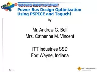
Power Bus Design Optimization Using PSPICE and Taguchi. by Mr. Andrew G. Bell Mrs. Catherine M. Vincent ITT Industries SSD Fort Wayne, Indiana. Rochester, NY (HQ). Fort Wayne, IN. Clifton, NJ. Vienna, VA. Boulder, CO. Introduction. ITT Space Systems Division (SSD)

Power Bus Design Optimization Using PSPICE and Taguchi
E N D
Presentation Transcript
Power Bus Design Optimization Using PSPICE and Taguchi by Mr. Andrew G. Bell Mrs. Catherine M. Vincent ITT Industries SSD Fort Wayne, Indiana
Rochester, NY (HQ) Fort Wayne, IN Clifton, NJ Vienna, VA Boulder, CO Introduction • ITT Space Systems Division (SSD) • Rochester, New York • Fort Wayne, Indiana • Clifton, New Jersey • Boulder, Colorado • Vienna, Virginia • 2,474 employees
Products Intelligence, Surveillance and Reconnaissance (ISR) Image Information Space Science and Commercial Remote Sensing Meteorological and Navigational Space Payloads Topic Optimization process for power busses Introduction
Objectives and Benefits • Objectives • Power Bus optimization using • Analysis of Means “ANOM” (Taguchi) • PSPICE running in a batch mode • Benefits • Optimization ensures highest quality design for the customer • Cost reduction by saving time
Approach • Use Analysis of Means (ANOM) • L18 orthogonal array for eight control factors • L4 orthogonal array for three noise factors • Use the smaller-the-better signal to noise ratio • Run simulations in a batch mode using PSPICE • Perform confirmation runs to evaluate optimal solution
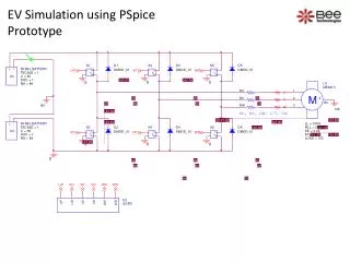
Example Power Bus Minimize both inrush current and output voltage drop length & wire gauge Baseline Performance: Inrush Current 19.16A Output Voltage Drop 1.18V Noise Factors Control Factors
Experimental Layout • Control Factor L18 OA • Noise Factor L4 OA • One experiment for inrush current • One experiment for output voltage drop • STB (Smaller the Better Optimization)
Smaller Best S/N Calculation: Inrush Current yi = each value determined for each run n = 4 (four groups run for each of the 18 runs)
Smaller Best S/N Calculation: Output Voltage Drop yi = each value determined for each run n = 4 (four groups run for each of the 18 runs)
Factor Level Average Graphs (ANOM) Factor Effect Plot Inrush Current Factor Effect Plot Output Voltage Drop
Confirmation Trials • Build 3 simulation schematics for each of the noise factor settings • Do comparison of inrush current and output voltage drop for best combination STB • Record optimization results for combination STB, Current STB and Voltage STB
Confirmation Trial Results output voltage drop inrush current • Largest S/N ratio for inrush current (-23.8dB) is Conf-I • Largest S/N ratio for output voltage drop • (-4.49dB) is Conf-V • Best S/N compromise for inrush current • (-23.83dB) and output voltage drop (-4.61dB) is Conf-Comb -23.80dB = 14.3A -23.83dB = 14.4A -25.90dB = 18.8A -4.49dB = 1.48V -4.61dB = 1.50V -4.89dB = 1.55V
Conclusions and Benefits • Optimal power bus design in less time and reduced cost • PSPICE in batch mode reduces simulation time and reduces cost • ANOM determines optimal control factor settings for best design
Acknowledgements • Thanks to • Eric Smith • George Adamczyk