DCS status
DCS status. DCS overview Implementation Examples DCS board ---> KIP DIM @ HD ---> Worms Open issues. DCS overview. Hirachical structure Front end configuration via DCS Monitoring Trigger distribution (hardwarewise). DCS implementation. Layered structure

DCS status
E N D
Presentation Transcript
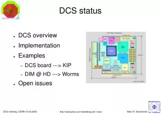
DCS status • DCS overview • Implementation • Examples • DCS board ---> KIP • DIM @ HD ---> Worms • Open issues
DCS overview • Hirachical structure • Front end configuration via DCS • Monitoring • Trigger distribution (hardwarewise)
DCS implementation • Layered structure • Supervisory layer = PVSS(DIM + (OPC)), DIM DNS... • Network layer = easynet + switches -> optics • Control layer = DCS board + DIM • Detector layer = scsb + JTAG
DCS Board • Design freeze • First prototype April • ARM processor based technology • 100k FPGA flexibility • 32MB RAM • LINUX system
Next steps • Interface to LV/HV supplies • Interface to Cooling • Interface to Gas system • OPC Server on Telemecanique PLC (at the moment) • Implementation in PVSS using FSMs
Introduction • DCS-board status report
DCS board • emergency handling • shutdown • JTAG-recovery (FPGA, FLASH ROM) • ADC possibilities: • measurement of power bar voltages • Temperature • Humidity sensor • Power up/down • MCM setup (initialisation, pedestal setting, and storing) • clock distribution (TTCrx) • Trigger distribution (TTCrx) • ethernet interface • testing tools: merger/MCM testing (LVDS)
DCS on the chamber Eight read-out boards controlled by one DCS board MCM setup (initialisation, pedestal setting, and storing) clock distribution (TTCrx) Trigger distribution (TTCrx) testing tool: merger/MCM testing (LVDS)
DCS Interfaces Optical clock receiver link (TTCrx) Ethernet link JTAG in/out 8 analog Inputs 16bit/10Sps 8 pseudo LVDS inputs and outputs 24 switching lines UART I2C Autonomous power Optional • CMC connector • Two 8 bit port
DCS functional Block Altera FPGA with ARM core and 100k gates Ethernet phsical layer chip 32 MByte SDRAM 16 Mbyte flash EPROM TTCrx clock recovery 3.3 and 1.8 Volt coltage regulators RS422 driver and receiver for JTAG LVDS clock and trigger driver Watchdog and Voltage Supervisor 16 (24) Bit ADC with 10 Samples per second
JTAG Fault Recovery DCS JTAG revitalization system: JTAG master implemented on each DCS-board. Dedicated JTAG loop to repair inconsistent program or configuration data of adjacent DCS boards.
Board Layout Size: 100 x 120mm Height: 10.5 mm max.
DCS board status • TPC will use the same DCS-board • design freeze • DCS-board routed with 8 layers (6 layers????) • April first prototype • working document: http://www.kip.uni-heidelberg.de/ti/DCS-Board/current/index.html
NIOS with scsb • Connection to MCMs • Slow control serial bus (scsb)
TRAP prototype • TRAP chip prototype • Positve test with scsb • Positive test with scsb
Work in progress • Porting uClinux to the CIA-board (Cluster Interface Adapter) • Testboard for the Intel PHY for EPXA-dev-board • Porting Linux to the DCS board • Porting the device driver to Linux on ARM-processor