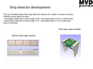
Micro strip detector development
This document outlines the development and manufacturing processes of micro-strip detectors for the CBM (Compressed Baryonic Matter) project. It provides insights into the initial runs of detector production, detailing the design specifications, performance results, and challenges encountered, particularly in breakdown voltage and capacitance issues. Further improvements through technology modifications are proposed. The findings include IV and CV test results, emphasizing design refinements needed for enhanced efficiency and radiation hardness. Future manufacturing plans within the INNOWATT project are also discussed.

Micro strip detector development
E N D
Presentation Transcript
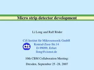
Micro strip detector development Li Long and Ralf Röder CiS Institut für Mikrosensorik GmbH Konrad-Zuse-Str.14 D-99099, Erfurt llong@cismst.de 10th CBM Collaboration Meeting: Dresden, September 25 -28, 2007
Outline The design of CBM detector The process of CBM detector Results: IV, CV of detectors The analysis of test structures Further development Simulation The layout for second iteration Contents
Status The first run of CBM detector manufacture: We have started 2 bathes of CBM detector manufacture. 50% of the first batch are finished and detectors are delivered. The rest of the wafers are processed to implantation step and waiting for the feedback of final test of the finished chips. • The first test results of finished detectors show: • The performance (full depletion voltage and dark current) of full size • detector and small baby detectors is OK, the middle size baby detector • has problem. • 2. Further improvement of breakdown voltage can be achieved by • technology modification. • 3. A refinement on design regarding interstrip capacitance, coupling • capacitance and irradiation hardness needs detailed tests with real • packaging and readout. Status
The design of CBM detector • . Double side micro strip silicon detector 2. Punch through biasing 3. Junction side: 15° stereo angle, double metallization, Multi guard. 4. Ohmic side: 90° stereo angle, P-spray isolation. 5. Three different types of detector, unit in µm Main features
The design of CBM detector Wafer layout
The design of CBM detector Chip list
The process of CBM detector 1. Punch through (7, 10, 13, 16µ) 2. Field plate (2, 0, -2µ) Test structures
The process of CBM detector Material applied: n-Si <111> 4~6kOhmcm, 285µm Double side polished Double side metallization is developed and introduced to the production line. The other process steps are standard for irradiation detector. Yield process
The process of CBM detector 1. CBM_01 Detector front side 2. CBM_01 Detector back side Photos
Results: IV, CV of detectors The IV curves of detectors form Wafer #7 (The dark current of bias ring with guard rings floating) Active area: SD=27.5cm2, SB1=4.2cm2, SB2~B5=1.7cm2 Dark current of D at operation bias ~10nA/cm2, at 300V < 1µA. IV
Results: IV, CV of detectors The C-2 ~v curve of full detector from Wafer #7 (The capacitance of bias ring with guard rings floating is measured) Full depletion voltage 53.8V r=4.9kOhmcm CV
The analysis of test structure Flat band voltage: Vfb -> qox qox=CiVfb Surface generation current Iox->S0 Iox=qniS0Ag The leakage current vs gate voltage at different bias can be measured. We can obtain the flat band voltage and surface generation current. From these we can calculate the oxide charge, interface recombination velocity. Gate diode
The analysis of test structure The effect of dicing edge
The analysis of test structure This group of test structure has 6 resistors with different width s = A + B*x Rsq= 107Ohm Conductance as a function of resistance path width Front side
Further development In frame of INNOWATT project “SPID “, we are planning the second run of manufacture to test more possibilities. Status: simulation & layout finished. Bias method: Punch through, Poly-silicon Breakdown voltage: Charge, Micro discharge Isolation technology: pspray , pstop, field plate The effect of dicing edge
Simulation Width=5µ, 235 Square. Bias resistance 1MOhm->4.3k Ohm /Sq For double side strip detector, one side of coupling capacitance must sustain the operation voltage. Since large coupling capacitance is preferred, thin oxide will be used, which may breakdown before the pn-junction breakdown. 300V breakdown voltage is enough. Poly silicon resistor
Simulation Field distribution of junction side
Simulation Field distribution ofOhmic side
Design Front side
Design Back side
Design A baby detector with pstop
Technology • .Starting material • .Oxidation and mark on FS and BS • .Etching and active zone on FS and BS • .Pstop (optional) • .Anneal • .Nitride and LTO deposition on FS and BS • .Patterning LTO on FS and BS • .Patterning Nitride on FS and BS • .Poly-silicon • .Protect FS for p-spray-Implantation in BS • .Activation anneal • .Contact hole on FS and BS • .Deposition AlSi FS and BS, AlSi Patterning FS and BS • .Deposition and patterning SiO2-Via FS, Deposition and patterning Si3N4-Passivation BS • .Deposition AlSi FS, AlSi Patterning FS • .Deposition Si3N4-Passivation FS, Patterning of Passivation FS Process flow
Technology Technology simulation: resistance for p front 66kOhm/cm resistance for n back 44kOhm/cm Layout calculation: coupling capacitance front 21pF/cm coupling capacitance back 15pF/cm resistance for front metal 25Ohm/cm resistance for back metal 16Ohm/cm resistance for cross connection 28Ohm/cm Electrical parameters