Download
1 / 10
100 likes | 214 Views
This study explores the effects of pipelining on signal accuracy and propagation delays in circuits. It addresses both passive and active circuit noise, emphasizing how circuit design influences signal integrity. A pipelined Fibonacci simulator is proposed to evaluate model order reductions while assessing different circuit designs and simulation setups. Results reveal sensitivity to current fluctuations, particularly in initial stages. Despite identified variances in delay, pipelining shows minimal improvement in performance under certain conditions, highlighting challenges in achieving signal predictability.

E N D
The Effects of Pipelining on Signal Accuracy and Propagation Delay Ammon Hardcastle Advisor Dr. Ken Stevens
Overview • Problem • Passive circuit noise • Active circuit noise • Test circuit qualifications • Circuit design • Simulation setup • Results • Conclusion
Passive Circuit Noise • Passive circuit elements: resistors, capacitors and inductors • Clean signal • Resistor and capacitor (RC) • Resistor, capacitor and inductor (RLC)
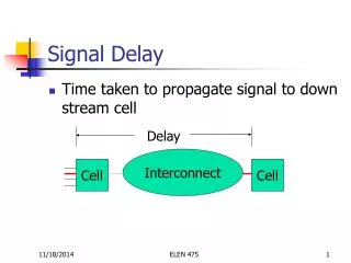
Active Circuit Noise • Active circuit elements: transistors • Saturation current • Triode current • Non-ideal transistor switching • Signal integrity • Signal propagation
Proposed Test • Design a pipelined Fibonacci simulator • Used to test the accuracy of the model order reductions of the two phase algorithm • 3 desired qualities • RLC separate from circuit • Passive vs. Active noise • Pipelined • Signals can be evaluated throughout the circuit • Signal locations are known throughout the circuit • Testable • Signals are predictable
Circuit Design • Fibonacci: Starting at stage 6 (8 13 21 34...) • 4 circuit designs: • 1 Stage (8 21) • 4 Stages (8 89) • 8 Stages (8 610) • 16 Stages (8 28, 657) • Power In • Micron Single Layer Package • Power Out 13 28,657 610 89 21 16-Bit Adder 16-Bit Register 8
Simulation Setup • Purpose of simulations • Determine accuracy of propagating signals • Compare differences between simulators • 3 test simulation • Control • HSPICE • Ideal power 1.2V (No Noise) • Single voltage source through package • HSPICE and HSimPlus • Independent voltage sources through package • HSPICE and HSimPlus
Results • Single voltage source • HSPICE single • Independent voltage sources • HSPICE multiple vs. Single vs. Ideal • Single voltage source • HSimPlus vs. HSPICE • Independent voltage sources • HSimPlus vs. HSPICE • Ideal voltage source • HSPICE
Results - Continued • Delay variation from control simulation Delay (pS) Stages Delay (pS) Stages
Conclusion • Power • IC designs sensitive to current fluctuations • 1st stage has the largest current variation • 1st stage has largest signal delays • Mean delay caused by noise decreases as the signal propagates • Multiple supplies have little affect on this circuit • Worst case improvement of only .5% • 6 cases with no improvement • Signal Propagation • Golden model underestimates actual delay • Variations up to 544pS (HSPICE) • HSimPlus vs. HSPICE • 1st stage delay only 50% of HSPICE • Largely underestimates noise affects for this circuit