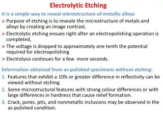
Electrolytic Etching
Electrolytic Etching. It is a simple way to reveal microstructure of metallic alloys Purpose of etching is to reveale the microstructure of metals and alloys by creating an image contrast. Electrolytic etching ensues right after an electropolishing operation is completed,

Electrolytic Etching
E N D
Presentation Transcript
Electrolytic Etching • It is a simple way to reveal microstructureof metallic alloys • Purpose of etching is to reveale the microstructure of metals and alloys by creating an image contrast. • Electrolytic etching ensues right after an electropolishing operation is completed, • The voltage is dropped to approximately one tenth the potential required for electropolishing • Electrolysis continues for a few more seconds. Information obtained from as-polished specimens without etching: Features that exhibit a 10% or greater difference in reflectivity can be viewed without etching. Some microstructural features with strong colour differences or with large differences in hardness that cause relief formation. Crack, pores, pits, and nonmetallic inclusions may be observed in the as-polished condition.
Toproduce an image contrast does not always refer to the selective chemical dissolution of various structural features. • Metallographic contrasting methods include; • electrochemical, • optical, and • physical etching techniques. Although use of etching is primarily intended for optical examination, polished and etched sections are increasingly examined using the scanning electron microscope with magnifications between those of the optical and transmission electron microscopes.
Methods of Metallographic Etching Nondestructive techniques, which do not alter the surface of the microsection: It includes optical etching and interference layers that are physically deposited on the surfaces of polished specimens. Destructive methods, which induce surface changes. 1. Nondestructive techniques Opticaletching techniques are; Dark-field illumination, Polarized light microscopy, Phase contrast microscopy, and Differential interference contrast, all of which use the Köhlerillumination principle known from the most common bright-field illumination mode.
The Köhler principle Fig. 1 The Köhler illumination principle in incident light microscopy
Some Particulars for Köhler Principle • Providesthe uniform illumination of the microsection necessary for obtaining optimumcontrast by optical etching. • The collector lens forms an image of the light source at the first condenser lens or at theillumination condenser aperture. • The second condenser lens reproduces the image of the light source in the back focalplane of the objective lens after reflection of the light at the reflector (plane glass, half-silvered mirror, or prism). • Therefore, the surface of the specimen is uniformly illuminated. The condenser lenses and the objective form an image ofthe radiant field stop in the plane of the specimen surface.
Dark-Field Illumination. • If the difference between the angle of incidence and half the aperture of the cone of light islarger than half the aperture angle of the objective, no regularly reflected light passes through the objective. • This isrealized in dark-field illumination (Fig. 2). Only those light rays deflected by diffuse scattering from their originaldirection toward the optical axis of the microscope are used for image formation. • Therefore, surface regions perpendicularto the optical axis will appear dark, and angled surfaces will appear light. • Dark-field illumination produces contrastcompletely reversed from that obtained using bright-field illumination. • Optical etching by dark-field illumination is applied to reveal cracks, pores, voids, and inclusions. Nonmetallic inclusionsoften undergo an intensive brightening by dark-field illumination. • The surface quality of polished microsections can alsobe controlled using this method, because even very fine scratches and indications of relief formation are revealed.
Polarized Light.The basic arrangement for optical etching by polarized light is shown in Fig. 3. Fig. 4 Grains and deformation twins revealed by polarized light on an as-polished section of cast bismuth. 50× Fig. 3 Principles of polarizedlight microscopy
Basic Principles: • The incident light onthe specimen is plane polarized by placing a polarizer in front of the condenser lens. • The reflected light is analyzed by apolarizing unit placed behind the eyepiece of the microscope. • This analyzer is normally in a crossed relationshipregarding the polarizer, with the plane of polarization of the analyzer perpendicular to that of the polarizer. • Application of this optical etching technique is based on the fact that optically anisotropic metals and phases reflect planepolarizedlight as elliptically polarized light with a rotation of the plane of polarization. • However, plane-polarized lightreflected from the surface of an optically isotropic cubic metal remains unchanged if it strikes at normal incidence.
Underthis condition, as-polished cubic metals will appear uniformly dark under crossed polars, because an analyzer in thecrossed position will extinguish the unchanged reflected beam. • By contrast, anisotropic metals and phases react topolarized light and exhibit a grain contrast effect under crossed polars as a variation in brightness and color. • Requirements for good results: • well-polished microsection, because surface irregularities, smudges, andsurface layers influence the state of polarization and may suppress anisotropic effects. • Chemical and electrolyticpolishing, because they avoid plastic deformation of the surface regions, are more successful than mechanical polishing. • Where used ? • Optical etching by polarized light is applied to anisotropic metals and to metal alloys containing anisotropic phases. • for revealing grain structure (Fig. 4) and for distinguishing and identifying phases inmultiphase alloys.
Detecting preferred orientation in polycrystalline materials and • Identifyingnonmetallic anisotropic inclusions in optically isotropicmetal-matrix materials. • Anisotropic surface layers produced by chemical etching or by anodic oxidation of isotropic metals and metal alloysprovide a stronger grain contrast when polarized light is used. • For anisotropic material, an increase in grain contrast isobserved when the surface of the polished microsection is coated with interference layers before examination underpolarized light. • A special application is the examination of polished cross sections of transparent resin, glass, or ceramiclayers. Under polarized light, the distinctive colors of these layers can be determined, and cracks or other flaws are revealed.
Phase ContrastMicroscopy. • Slight differences in height on polished microsections are invisible in bright-field illumination,because they produce only phase differences between the reflected light waves. • Optical etching using the phase-contrasttechnique transforms these phase differences into detectable variations in brightness. • To achieve phase contrast, anangular disk is inserted at the front focal plane of the condenser lens, and a transparent phase plate of suitable size isplaced in the back focal plane of the objective, as shown in Fig. 5. • Depending on the type of transparent phase plate used,positive or negative phase contrast results. In positive phase contrast, higher areas of the specimen appear bright, anddepressions dark. In negative phase contrast, lower areas on the specimen are brighter, and higher areas are darker thanthe background. • Minimal differences in height of 1-5 nm (10-50 Ao ) are disclosed using this method. The optimumrange of differences in surface level is approximately 20-50 nm 200-500 Ao).
Where Used • The phase-contrast technique can be applied to reveal the microstructure of metals and alloys after polishing or lightetching of the microsections. • Examplesinclude (1) the identification of carbide and σ phase in ferritic chromium steel and (2) theidentification of σ phase in austenite. • Other applications of phase-contrast microscopy include the study of cleavagesurfaces and the observation of twins and slip lines. • It is also useful as an optical etching method in high temperature • (hot-stage) microscopy.
Differential Interference Contrast. • How it works? • Differentialinterference contrast after Nomarski has found broad application in metallography. The basic arrangement for this opticaletching method is shown in Fig. 6. • A ray of light emitted from the light source is linearly polarized after it passes throughthe polarizer. • The polirized light then enters the Nomarskibiprism (Wollaston prism), which consists of two optically uniaxially doublyrefracting crystals and is divided into two rays of linearly polarized light. • The planes of vibration of these rays areperpendicular to each other. • Upon passing through the objective, the rays become parallel and impinge on the specimen.After reflection from the specimen surface, they are recombined by the biprism. • Interference is produced when theserecombined rays pass through the analyzer.
Fig. 6 Principles of differential interference contrast after Nomarski
How it function? • Likenormal polarized light microscopy, the analyzer is in a crossed relationship with respect to the polarizer. • Phasedifferences resulting from the two spatially separated beams reflecting from the specimen are due to differences in heightof the surface relief, which are modified by the optical properties of the specimen. • These phase differences cause thelight-dark or color interference contrast. Lateral displacement of the biprism allows an additional phase difference to besuperimposed that varies color contrast. • The achievable contrast depends on the local gradient of the phase difference.Therefore, this type of contrast is termed differential interference contrast.
Where used? • To reveal phases of different hardness in polished microsections of metalalloys, layered materials, and materials joints. • Tovisualize carbide particles in rollerbearing and highspeed steels. • To study the coherent phase transformations, which producesurface reliefs. • Todetect surface and subsurface defects of thin films evaporated or sputtered on metallic or nonmetallic substrates Fig. 7 Differential interference contrast after Nomarski showing the two-phase structure of a U-33Al-25Co(at.%) alloy. Electrolytically etched. 250×
Contrasting by Interference Layers (Principles). • The method of revealing the microstructure with the aid of physicallydeposited interference layers (films) is based on an optical-contrast mechanism without chemical or morphologicalalteration of the specimen surface. • The specimen is coated with a transparent layer whose thickness is small compared tothe resolving power of the optical microscope. • In interference layer microscopy, light that is incident on the depositedfilm is reflected at the air/layer and layer/specimen interfaces (Fig. 8). • Phases with different optical constants appear invarious degrees of brightness and colors. • The color of a phase is determined by its optical constants and by the thicknessand optical constants of the interference layer. • How layers are deposited? Reactively sputtered and vapor-deposited films are used as an interference layers.
Fig. 8 The function of a physically deposited interference layer. Contrast between phase A and B is achieved byoptimizing the optical constants (ns: refractive indices, ks: absorption coefficients) of the layer with respect to the optical constants of the phases (nA, kA,nB, kB) and adjusting the layer thickness ds.
The optimum contrasting conditions is achieved simply by a commercially available contrasting chamber where the results of reactive sputtering can be directly observed by placing the coated specimen under a microscope without removing the specimen from the chamber (see Fig. 9). The chamber consists of an atomizer with interchangeable cathodes, a high-voltage supply, and an electron gun to ionize the reactive gas (oxygen). Fig. 9 Gas contrasting chamber used for reactive sputtering and optical examination of interference layers onpolished specimens. The results of the reactive sputtering process can be monitored through the viewingwindow.
Reproducible results can be maintained when the polished microsection is carefully prepared. • This technique is applied to various metal alloys, composite materials, coatings, and joined materials. For example, good contrast is obtained for aluminium alloys, high-temperature nickel and cobalt alloys, cemented carbides, plasma-sprayed layers, brazed joints, and sintered metals. • Typical results of contrasting by interference layers are illustrated in Fig. 10; four phases can be differentiated on thepolished microsection of a cast tin-silver-copper alloy coated with a platinum oxide layer. Fig. 10 Interference-layer micrograph of a cast Sn-18Ag-15Cu alloy. Polished specimen coated with a platinumoxide layer by reactive sputtering. Structure consists of Ag3Sn (white), Sn (light gray), Cu6Sn5 (medium gray),and Cu3Sn (dark gray). 300×
Destructive Etching (Classification) • The types of destructive etching: (a) electrochemical and (b) physicaletching. • The classical electrochemical etching procedures, including conventional etching, are utilized more frequently than physical etching methods which are used primarily when other techniques fail. • Electrochemical (Chemical) Etching. • Main principles: • During the etching (a) cathodic and (b) anodic reactions take place. • All metals contacting the etching solutions tend tobecome ionized by releasing electrons. • The extent of this reaction can be recorded by measuring the electrochemicalpotential. • This is performed by comparing the potential of metal versus the standard potential of a reference electrode. • The tabulation of various metals results in the electromotive series of elements: Li+, Na+, K+, Ca++, Ba++, Be++, Mg++, Al+++, Mn++, Zn++, Cr+++, Cd++, Ti+, Co++, Ni+, Pb++, Fe+++, H+, Sn++++, Sb+++, Bi+++, As+++, Cu++, Ag+, Mg++, Au+++, Pt+++.
The elements in table are listed in decreasing electroaffinity. Acids attack all elements preceding hydrogen (H2) as it evolves. • All elements following hydrogen cannot be attacked without the addition of an oxidizing agent. • Microstructural parts of different electrochemical potential are attacked at varying rates, producing differential etchingrequired for microstructural contrast.Electrochemical etching can be considered "forced corrosion." • The difference in potential of the microstructural parts creates formation of mini micro-cells consisting of small, adjoining anodic and cathodic regions. • Types of inhomogeneities causing micro elements: • Differences in phase composition. • Irregularities present in the crystal such as at grain boundaries.
Inhomogeneities due to deformation (deformed zones), which are less resistant to attack than undeformed material • Inhomojenity in the formation of oxidation layers (regions free of oxides are preferentially etched) • Concentration fluctuation in the electrolyte (low concentration is less resistant) • Differences in electrolyte velocity (higher circulation rates reduce resistance to attack) • Differences in the oxygen content of the electrolyte (aerated solutions are more resistant) • Differences in the illumination intensity, which can initiate differences in potential • Because of differences in potential among microstructural features, dissolution of the surface proceeds at various rates,producing contrast.
Precipitation (Deposit) Etching. • Contrast can also originate from layers formed simultaneously with materialdissolution. • In precipitation etching, the material is dissolved at the surface; it then reacts with certain components of theetchant to form insoluble compounds. • These compounds precipitate selectively on the surface, causing interference colorsor heavy layers of an inherent color. Heat • Tinting. • Oxide films can be formed by heat tinting. The polished specimen is heated in an oxidizing atmosphere. • Coloration of the surface takes place at different rates according to the reaction characteristics of different microstructuralelements under the given conditions of atmosphere and temperature. The observed interference colors allow thedifferentiation of phases and grains.
Chemical etching • The oldest and most commonly applied technique for producing microstructural contrast. • In thistechnique, the etchant reacts with the specimen without the use of an external current supply. • Etching proceeds byselective dissolution according to the electrochemical characteristics of the microstructural constituents.
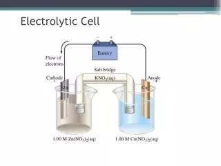
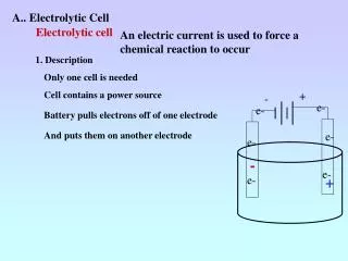
Electrolytic (anodic) Etching. • Electrical potential is applied to the specimen using an external circuit. • Figure 11 shows a typical setup consisting of the specimen (anode) and its counterelectrode (cathode) immersed in an electrolyte (etchant). • During electrolytic etching, positive metal ions leave the specimen surface and diffuse into theelectrolyte; an equivalent number of electrons remain in the material. • This results in direct etching, shown as segment AB of the current density versus voltage curve in Fig. 12. • Specimen dissolution without formation of a precipitated layer occurs in this instance. However, if the metal ions leaving the material react with nonmetal ions from the electrolyte and form an insoluble compound, precipitated layers will form on the specimen surface whose thicknesses are a function of the composition and orientation of the microstructural features exposed to the solution.
Fig. 11 Basic laboratory setup for electrolytic etching and polishing
Fig. 12 Idealized current density versus applied voltage for many common electrolytes. Regions for electrolyticetching and polishing are indicated.
Anodizing: • The formation of layers by electrolytic etching that reveal interference colors due to variations in thicknessdetermined by the underlying microstructure. • Zirconium and Hafnium and Their Alloys are good example for anodizing. • Potentiostatic etching: • An advanced form of electrolytic etching that produces the ultimate etching contrast throughhighly controlled conditions. • The potential of the specimen, which usually changes with variations in electrolyticconcentration, is maintained at a fixed level through the use of a potentiostat and suitable reference electrodes. • Theprinciple of this technique is shown in Fig. 13. In some cases, the cell current can be maintained with a coulombmeter todetermine the extent of etching (controlled etching).
Physical etching • The surface is free of chemical residues, • offers advantages where electrochemical etching is difficult--for example, when there is an extremely large difference in electrochemical potential between microstructural elements or when chemical etchants cause stains or residues that could produce false microstructures. • (1) Ionicetchingand (2) thermal etching are physical etching techniques that alter the morphology of the polished specimen surface. • Some probable applications of these methods are ceramic materials, plated layers, welds joining dissimilar materials, and porous materials. • (1) Ionicetching(or cathodic vacuum etching) • structural contrast is created by selective removal of atoms from thespecimen surfaceby using highenergyions, such as argon, accelerated by voltages of 1 to10 kV. • Individual atoms are removed at various rates,depending on their atomic number, their bonding state, andthe crystal orientation of the individual grains. • Ion beam etching and cathodic sputtering are the ion etching techniquesused in metallography and ceramography.
(2) Thermal etching • It is used in high-temperature microscopy and to etch polished surfaces of ceramic materials well belowtheir sintering or hot-pressing temperature. • Thermal etching is also partially based on atoms leaving the material surfaceas a result of additional energy. • However, the predominant force in thermal etching is the formation of slightly curvedequilibrium surfaces having individual grains with minimum surface tension. • Thermal etching of ceramic materials in air,vacuum, or inert gases is often better than conventional chemical etching. • Figure 14 shows as an example the grainstructure of a diffusion-welded ceramic joint revealed by thermal etching.
Fig. 14 Polished section of a diffusion-bonded joint between a coarse-grained and a fine-grained aluminaceramic (99.7% Al2O3) thermally etched in air at 1400 °C (2550 °F) for 1 h. 500×