Download
1 / 8
80 likes | 240 Views
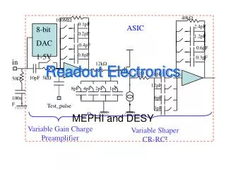
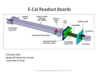
E-Cal Readout Boards. - 8 Boards total Design & Fabrication at Jlab Assembly at Orsay. MotherBoard. 4 Boards (2-Identical) 16- layers 6 signal layers 2 High Voltage 2 Low Voltage 6 Ground. Each Signal trace has Ground guard traces Signal trace 8mil space 8 mil

E N D
E-Cal Readout Boards • - 8 Boards total • Design & Fabrication at Jlab • Assembly at Orsay Nick Nganga HPS Collaboration Oct 18-19 2011 - Jlab
MotherBoard • 4 Boards (2-Identical) • 16- layers • 6 signal layers • 2 High Voltage • 2 Low Voltage • 6 Ground • Each Signal trace has Ground guard traces • Signal trace 8mil space 8 mil • Stackup verified in BoardSim • Crosstalk simulated for longest traces • **Board layers for Full Experiment. Nick Nganga HPS Collaboration Oct 18-19 2011 - Jlab
Connection Boards • 4 Boards (2 similar) • 2 Layers • 2 Connectors (No traces) APD Connections (2 pins) Anode Cathode Amplifier Connections GND (2 pins) High Voltage (1 Pin) Nick Nganga HPS Collaboration Oct 18-19 2011 - Jlab
Ecal Grouping Each grouping requires its own High Voltage Connection Nick Nganga HPS Collaboration Oct 18-19 2011 - Jlab
SI - Simulation Characteristic Amplifier Output (DVCS 2005) Tested on Longest Trace ~ 22inches Equivalent to 4ns prop. delay. Nick Nganga HPS Collaboration Oct 18-19 2011 - Jlab Longest Trace Highlighted for Signal Integrity Analysis
Simulation Setup: CMOS Driver with 0.8V/ns slew rate. Termination: 50-ohm. Result: Less than 2% reflection (40mV on 2V scale) Nick Nganga HPS Collaboration Oct 18-19 2011 - Jlab
CROSSTALK SIMULATION Crosstalk Threshold set to 15mV (only one trace affected) Crosstalk Threshold set to 20mV (Two traces affected) Nick Nganga HPS Collaboration Oct 18-19 2011 - Jlab
Board Status (design) • Connection Boards ~1.5 Days • Bottom Right ~0.5 days • Top Right ~ 0.5 days • Bottom Left, Top Left ~ 0.5-day • MotherBoards ~2.5 Days • Bottom Right ~1 day • Top Right ~ 1 days • Bottom Left, Top Left ~ 0.5-days Nick Nganga HPS Collaboration Oct 18-19 2011 - Jlab