Download
1 / 64
640 likes | 819 Views
This presentation outlines a comprehensive project focused on designing and implementing an ECG application using FPGA technology over two semesters. It covers the heart's electrical impulses analysis vital for diagnosing heart diseases. The project includes creating a communication interface between a PC and an ECG board, developing a simulation component for testing, and building an interactive GUI with debugging capabilities. The architecture integrates with various components, ensuring performance and reliability for continuous heart monitoring. Key challenges faced during development and conclusions drawn are also discussed.

E N D
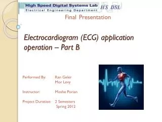
Electrocardiogram (ECG) application operation – Part B FinalPresentation Performed By: Ran Geler Mor Levy Instructor: Moshe Porian Project Duration: 2 Semesters Spring 2012
Contents • Introduction • Overview • Top Architecture • Components • Data Flow • Simulations and Debug • Performance • GUI • Problems in developing process • Conclusions
Introduction • The heart is a muscular organ that beats in rhythm to pump blood through the body • By analyzing the heart behavior and especially the electrical impulses we can help identify heart diseases and special circumstance that require close monitoring
Medical Terms • ECG • Lead • Bipolar leads • Unipolar leads • Precordial Leads
Project Overview Project focus
Project Goals • Design and implement a communication interface between a PC to an ECG board using a FPGA. • Implement a simulation component to PCB board behavior for tests. • Learn how to integrate Multi Platforms elements • ECG DB with FPGA • Build an interactive GUI with debugger abilities. • Methodic project
What we have achieved: • Implementing ECG controller • ECG FSM • Integration with peripheral components. • Examination of the Implemented components • Creating tests bench • Mocking TI DB behavior • P & R to projects top architecture by Quartus • Adding Flash memory support • Implementing a GUI
Top Architecture – Frequency Frequency requirements for modules MATLAB GUI: Rx / Tx Via UART interface @ frequency of 115,200Hz FPGA: Main frequency: 100MHz Rx / Tx Modules @ frequency of 115,200Hz ADS1928R: Main frequency: 2.048MHz SPI-Data Out freq’: >110KHz Flash Memory: Main frequency: 100MHz
Core microarchitecture Data Rate: 100MHz 512Bytes Data Rate: >110KHz
Core Architecture • ECG FSM • FIFO • Command & Aux Regs • Wishbone Master & Slave • SPI Cores
ECG FSM • Controls the flow of data between the host and the DB • Three Main chain of actions: • Read Data • Read Registers • Write Registers
FIFO at ECG Controller • FIFO Size: 512 Bytes. • Stores Instruction and Sampled data. • Data structure on Instruction case: 1st Command 2nd Command Operation Commands (ex: RDATAC, Rreg, Wreg, Standby, Reset, ect’..) Additional Data Optional: Second Byte for (Rreg, Wreg) and sample interval for RDATAC command. Data for commands
SPI • The SPI Interface frequency: • At 24bit resolution per 8 Electrodes and 500 Samples per Sec: • Active at low. i.e. CS = ‘0’
Flash Component WBS Flash Component FLASH Flash FSM Flash Controller RAM 256Byte Reset en
Flash Component - Flash • One sample(24bit res. per 8 Electrodes)= 27Byte. • Lets assume sample rate of 500 SPS • Flash size = 4MB • Therefore we can sample for 5min.
Flash Component – Flash client BUS Technical Demands: • Common FLASH Interface protocol (CFI) • Wishbone Interface • Performs Read, Write, Reset and Erase transactions • Initiative read on power-on • Contains a timeout algorithm • Generic: adaptable to different FLASH sizes and clock frequencies. CFI Wishbone
ADS1298R ECG DB • FPGA Architecture design suited to Texas Instruments ADS1298R board. • Arrived to the High Speed Digital Systems Lab
Test Methodologies • Operation of the ECG Controller: • Checking that states change are at time • Checking control signals & data signals between units • Non existing commands • Read\Write data to flash from all components. • Read\Write data from PC to board simulation component (DB Mock). • NOTE: When a transaction is executed the wishbone “stall” signal is raised to ‘High’, So other requests will remain pending at the Rx Wishbone Master.
ECG Controller TB Data Flow • We have implemented a special closed component for Testing.
DB Mocking • We have implemented a component to imitate the Texas Instruments ADS1298R Chip behavior. • The Mocking component is capable ofsaving 26 configuration registers values. • Extracting \ writing data from a sequence ofregisters in a burst. • Simulate a continues samples reading (RDATAC mode).
DB mocking • The component designed to meet timing constrainsof Texas Instruments board. • Instructions and returned data timings. • Continues data samples timing. • Enter to sleep mode \ Wakeup time. • The component designed to help on Top architecture Implementation and debug process. • The component Interface is as the Texas Instruments boars (SPI).
Simulations – Read Transaction example • Top Architecture Wave. Flash Rx Transaction SPI
Simulations – Read Transaction example • SPI Transaction
Simulations – Read Transaction example • Flash transaction
Simulation equipment Programming & Debug gear Host for Simulations DE2 -Board
Quartus Simulations • Top Arc Synthesis summary
Quartus Simulations • Max Frequency • Architecture clocks
GUI • UsingMatlab 2012a we build a functional GUI • Allows control on the DB using the DB registers • Enables to communicate directly with the flash • Running ECG analyze