Download
1 / 16
180 likes | 300 Views
This chapter covers combinatorial circuit design, gate fan-in limits, gate delays, timing diagrams, hazards in logic, simulation, and testing. Includes design problems and figures. Learn to analyze and optimize logic circuits.

E N D
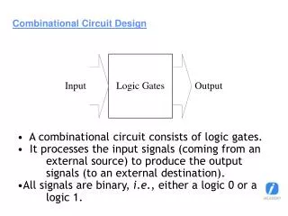
This chapter in the book includes: Objectives Study Guide 8.1 Review of Combinational Circuit Design 8.2 Design Circuits with Limited Gate Fan-In 8.3 Gate Delays and Timing Diagrams 8.4 Hazards in Combinational Logic 8.5 Simulation and Testing of Logic Circuits Problems Design Problems FIGURES FORCHAPTER 8COMBINATIONAL CIRCUIT DESIGN AND SIMULATION USING GATES Click the mouse to move to the next page. Use the ESC key to exit this chapter.