CMOS Circuit Design, Layout and Simulation
270 likes | 1.1k Views
CMOS Circuit Design, Layout and Simulation. Sam Burke UCSB HEP Group. References. Text CMOS Circuit Design, Layout, and Simulation by R. J. Baker, Li and Boyce IEEE Press Oct 2002 ISBN-81-203-1682-7 URL http://cmosedu.com/cmos1/book.htm. The Well. P Type Wafer

CMOS Circuit Design, Layout and Simulation
E N D
Presentation Transcript
CMOS Circuit Design, Layout and Simulation Sam Burke UCSB HEP Group
References • Text • CMOS Circuit Design, Layout, and Simulation by R. J. Baker, Li and Boyce IEEE Press Oct 2002 • ISBN-81-203-1682-7 • URL • http://cmosedu.com/cmos1/book.htm
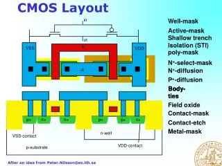
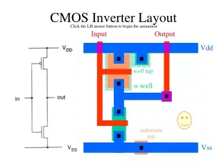
The Well • P Type Wafer • boron acceptor atoms (25 ohm*cm) • Transistors • Nmos Transistors on p-substrate • Pmos Transistors on n-well • Diode • formed between the n-well and p-substrate
Historical Methods • Point Contacts • 1948 • Grown Junctions • 1950 • Alloy Junctions • 1952 • Planar Technology or Junction Technology • 1953
Patterning • Start with clean bare wafer • Grow Oxide • wet oxide • dry oxide • Apply Resist • Photo-resist pattern • Expose • Develope • Etch to remove oxide • Ready for Diffusion
Growing an N-Well • Donor Atom Diffusion • Donor valance=5 • Phosphorus • Si valance=4 • N Well Resistivity • 0.75 ohm*cm
The Well Resistor • R=[p/t]*L/W • R=Resistance • p=resistivity • R=Rsq*L/W • Rsq=sheet resistance (ohm/square) • For N-Well • p=0.75ohm*cm • t=3um L=100um • W=10um • R=2500*100/10=25kohms
Si Resistivity • Experimental Data • N-Type donor concentration shown for resistor example • Ref: Grove, A.S “Physics and Tech - -
L-Edit • Demo the creation of an N-Well using L-Edit • Error checking
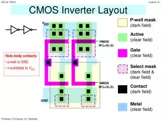
Well and Contacts • N-Well contact on left • metal1 • active • Bulk contact on right • metal1 • active • P Implant
PN Junction Depletion • Carrier drift