Combinational Circuit
Combinational Circuit. Yan Gu. 2 nd Presentation for CS 6260. What is Combinational Circuits?. Combinational Circuits refers to a family of models of computations.

Combinational Circuit
E N D
Presentation Transcript
Combinational Circuit Yan Gu 2nd Presentation for CS 6260
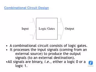
What is Combinational Circuits? Combinational Circuits refers to a family of models of computations. in general terms, a combinational circuit is defined as a device taking a number of inputs at one end and producing a number of outputs at the other end.
features • combinational circuit is made up of a number of interconnected components arranged in columns called stages. each component can be viewed as a simple processor. It has a constant fan-in----- that is , a constant number of input lines. These lines carry data from the outside world or from a constant number of components in a previous stage. each component also has a constant fan-out-------- that is , a constant number of components in a subsequent stage. • each component, having received its inputs, computes a certain function of these inputs in one time unit and produces the result as output. • No feedback: no component can be used more than once while computing the circuit’s output for a given input • The Size of a combinational circuit is defined as the number of components it uses. The depth is the number of stages in the circuit----- that is , the maximum number of components on a path from input to output. The Width of a circuit is the maximum number of components in a stage. The product of the depth and width provides an upper bound on the size of the circuit.
Depth and Width of a combinational circuit: Input Width Output . . . . . . Depth
An omega circuit 1 2 3 0 0 1 1 2 2 Row 3 3 4 4 5 5 6 6 7 7 An omega circuit, has n inputs and n outputs, it consists of logn columns (stages), numbered 1,2, …,logn from left to right, with n rows (input and out lines) per column, numbered 0,1,…, n-1 from top to bottom. There are n/2 processors per stage, each with two input and two output lines .the processors in stage j are connected to those in stage j+1, j=1,2,…,(logn)-1, by a perfect-shuffle interconnection. Thus, output line I in stage j is connected to input line 2i in stage j+1, for 1=<i=<(n/2)-1, and to input line 2i+1-n in stage j+1, for (n/2)=<i=<n-1. the circuit has a depth of logn, a width of n/2, and a size of (n/2)logn. In this example of figure, n=8
A butterfly circuit 3 0 1 2 0 1 2 3 Row 4 5 6 7 Butterfly circuit, has n inputs and n outputs, it consists of 1+logn columns, number 0,1,…,logn,whith n rows per column, numbered 0,1,…,n-1.let P(i,j) represent the processor in row i and column j. for 0=<j<logn, P(i,j) is connected to P(i, j+1) and P(k,j+1), where the binary representations of i and k Differ only in their jth least significant bit. The circuit has a depth of 1+logn, a width of n, and a size of n+nlogn. In the example of figure , n=8.
A merging circuit 2 1 4 2 7 3 8 4 1 5 3 6 5 7 6 8 a Merging circuit receives as input two sequences of data, each consisting of n/2 values sorted in nondecreasing order. It produces as output these two sequence combined into a single sequence of n data values sorted in nondecreasing order. One such circuit, known as the odd-even merging circuit, is shown for n =8. it consists of logn stages, with at most n/2 processors per stage. each processor is a comparator :it receives two values as input and produces the smaller of the two on its top output line and larger on the bottom line. The circuit has a depth of logn, a width of n/2, and a size of 1+(n/2)x((logn)-1).
An odd-even-merge sorting circuit 4 1 8 2 3 7 2 4 5 1 5 6 7 6 3 8 A sorting circuit receives as input a sequence of ndata values and produces as output these same data values arranged in nondecreasing order.one such circuit, know as the odd-even-merge sorting circuit is shown in the figure, it consists of O(logn) stages, with at most n/2 processor per stage. Each processor is a comparator . The circuit has a depth of O(logn), a width of O(n), and a size of O(nlogn).
Outputs (n) A (theoretically) efficient sorting circuit 1 1 Inputs (n) 2 1 2 4 2 4 2 4 3 3 8 1 3 4 7 3 4 2 8 5 1 5 5 5 7 6 6 6 5 6 3 6 8 7 7 7 8 8 A (theoretically) efficient sorting circuit consists of a complete tree with leave, 1+logn levels. And a total of 2n-1 nodes. each nonleaf node is circuit made of comparators. The circuit in a node is capable of receiving a set of m numbers, 2=<m=<n, and splitting it into two sets: the node’s top child receives a set of m/2 numbers, each of which is smaller than or equal to the m/2 numbers st to the node’s bottom child. in this way, if n numbers in arbitray order are fed to the root as input, they emerge from the leaves sorted in nondecreasing order from top to bottom .this circuit, referred to as the sorting-by-splitting circuit, has a depth of O(logn), a widthof O(n), and a size of O(nlogn)
A memory access unit for the RAM U000 U001 U010 U011 U100 Processor U101 U110 Memory MAU U111 In the RAM, there is one processor and a memory consisting of M locations .the model allows the processor to specify an arbitrary memory location from which it wishes to read or to which it wishes to write. The job of the MAU is to set up a path from the processor to the chosen memory location. a MAU for the RAM can be implemented as a binary tree of switches. The tree’s root is connected to the processor, and each of the leaves to a distinct memory location. The tree has 1+logM stages, numbered 1, 2,..,1+logM, with the root at stage 1. the tree links are assumed to be two-way communication lines, a switch can therefore send or receive a datum to or from one of its children and parents. this MAU has depth O (logM) AND width O (M), since the tree has 2M -1 switches, its size is O(M.)
A naive MAU for the PRAM 1 2 3 U1 1 2 3 4 P1 1 2 3 U2 1 2 3 4 P2 1 2 3 U3 1 2 3 4 1 2 3 P3 U4 MAU M Memory Location Processor Tree Memory Location Tree In PRAM, there are N processor and M memory locations. The model allows each processor to specify an Arbitrary memory location to which it wishes to gain access. several processors are allowed to read from or Write into the same memory location. a MAU for the PRAM creates paths from the processors to the memory Location. Each processor is connected to the root of a binary tree with M leaves numbered 1 to M, and each Memory location U is connected to a binary tree with N leaves numbered 1 to N. the MAU has a width of O(N x M), a depth of O(logM + logN), and a size of O(N x M).
An efficient MAU for the PRAM U1 Sorting Circuit P1 U2 P2 . . . . . . . . . . . . PN UM Merging Circuit N Processors MAU M Memory Locations An efficient MAU for the PRAMconsists of a sorting circuit and a merging circuit, and the merging Circuit receives tow sorted list to be merged: one is the output of sorting circuit, and The second one is received from the shared memory. The merging circuit has no Output, take place the data inside. The MAU has a widthof O(m+n), a depthof O(logN)+O(log(M+N)), a size of O(NlogN)+O((M+N)log(M+N)).
Sorting Circuits A combinational circuit for solving the sorting problem is called sorting circuit.There are two approaches can be used to design the circuit for the sorting problem. 1. Sorting by merging The sequence to be sorted is divided into two subsequences of equal length. Each of the two subsequences is now sorted recursively, finally, the two sorted subsequences are merged into one sorted sequence. • Sorting by splitting the sequence to be sorted is divided into two subsequences of equal length such that each element of the first subsequence is smaller that or equal to each element of second subsequence .this splitting operation is the then applied to each of the two subsequence recursively. when the recursion terminates, the sequence is in sorted order.
Sorting by merging • The odd-even Merging circuit Assume to merge tow sorted sequences{x1, x2, …, xm} and {y1, y2, …, ym}, to form a single sorted sequence {z1, z2, …, z2m}. In general, a circuit for merging sequences{x1, x2, …, xm} and {y1, y2, …, ym} is obtained as follows: 1. The odd-indexed elements of the two sequences{x1, x3, …, xm-1} and {y1, y3, …, ym-1} are merged to produce a sorted sequence {u1, u2,…, um}. • simultaneously, The even-indexed elements of the two sequences{x2, x4, …, xm} and {y2, y4, …, ym} are merged to produce a sorted sequence {v1, v2,…, vm}. • Finally, the output sequence {z1, z2,…, z2m} is obtained from z1=u1, z2m =vm, z2i=min(ui+1, vi), and z2i+1=max(ui+1, vi), for i=1, 2, …, m-1
z1 z2 z3 … zm-1 zm zm+1 zm+2 zm+3 … z2m-1 z2m u1 u2 u3 … um-1 um v1 v2 v3 … vm-1 vm X1 X2 X3 … Xm-1 Xm Y1 Y2 Y3 … Ym-1 ym (m/2,m/2) Merging circuit … … (m/2,m/2) Merging circuit • An (m, m) odd-even merging circuitconsists of two(m/2, m/2)odd-even merging circuits, • Followed by a column of m-1 comparators, the two (m/2, m/2)merging circuit s are • obtained by applying the same construction recursively; that is: • Each (m/2, m/2)merging circuit views its input as two sequences , each indexed • from 1 to m/2. • 2. Each (m/2, m/2)merging circuit uses two (m/4,m/4) merging circuits, followed by a • column of (m/2)-1 comparators • An (m, m) odd-even merging circuit has the depth of O(logm), the width of O(m), the • Size of O(mlogm)
Reference: Parallel Computation (models and methods) Selim G. AKL
Questions: 1. What the Size of a Combinational Circuit? What is the Width and the Depth of a Combinational Circuit? 2. What is the an upper bound on the size of the circuit? Answers: 1. The Size is defined as the number of components it uses; The depth is the number of stages in the circuit----- that is , the maximum number of components on a path from input to output. The Width of a circuit is the maximum number of components in a stage. 2. The product of the depth and width provides an upper bound on the size of the circuit.