Download
1 / 14
140 likes | 255 Views
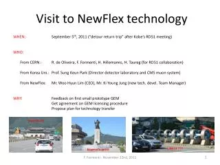
Visit to NewFlex technology. WHEN: September 5 th , 2011 (“detour return trip” after Kobe’s RD51 meeting) WHO: From CERN : R. de Oliveira, F. Formenti , H. Hillemanns , H. Taureg (for RD51 collaboration)

E N D
Visit to NewFlex technology • WHEN: September 5th, 2011 (“detour return trip” after Kobe’s RD51 meeting) • WHO: • From CERN : R. de Oliveira, F. Formenti, H. Hillemanns, H. Taureg (for RD51 collaboration) • From Korea Uni.: Prof. Sung Keun Park (Director detector laboratory and CMS muon system) • From NewFlex: Mr. Woo Hyun Lim (CEO), Mr. Ki Young Jung (new tech. devel. Team Manager) • WHY: Feedback on first small prototype GEM • Get agreement on GEM licensing procedure • Propose plan for technology transfer LINAC4 ??? Imperial city Emperor’s guard F. Formenti - November 22nd, 2011
NewFlex technology company Location: Asan, south west of Seoul, South Korea – about 1.5 hour by underground from Seoul center Size: 400 employees, 12500 m2 plant surface Production capacity: ~40000 m2 /month of Flexible PCB, ~ 30000 m2 /month of Metal PCB F. Formenti - November 22nd, 2011
Also part of NewFlex group (note: both of these companies not visited) NewCRETEC Location: Asan, next to NewFlex company Size: 1250 m2 plant surface Production capacity: ~6000 m2 /month of Flexible PCB Specialized in fine pitch, chip on board NewFlex subsidiary in China Location: Qingdao, Shandong province Production capacity: ~12000 m2 /month of Flexible PCB Being acquiring full process capability F. Formenti - November 22nd, 2011
NewFlex profile • - Established in 1992 (started as rigid PCB manufacturer) • Began Flexible PCB manufacturing in 1996 (15yrs experience) • NewCRETEC joined in 2009 • Target market application fields: • LCD displays • Touch screens • Cameras and portable camcorders • Laptops and PC peripherals • Automotive • Cellular phones • Flexible PCB commercial product ranges: • - Single side (70-120 µm thickness, 40 µm tracks) • - Double side (110-220 µm thickness, 50 µm tracks) • - Multi layer (3-8 layers, ≥250 µm thickness, 70 µm tracks) • Rigid-Flex (4-8 layers) • Sequential build up & inner via holes (4-8 layers) • Metal PCBs: • Semi rigid PCB with thick Cu tracks, • Used for power distribution, LED light sources Prof. Sung-Keun Park, Dir. Detect. Lab. Korea Uni. and CMS muon system Mr. Woo-Hyun Lim, NewFlex CEO F. Formenti - November 22nd, 2011
NewFlexproduction and R&D • Example of standard production schedule: • - Samples in less than 1 week • - Production setup from 2 to 3 weeks • Production minimal order claimed not a problem • (typically from industry 200 m2) • R&D on processes: • Embedded resistors (NiCr, low resistance ~10Ω/[], finite values range of units of kΩs) • Embedded capacitors (polyamide dielectric, low values, area limited) • Embedded optical waveguides (typ length 12 cm, attenuation 0.18dB/cm) • Silver ink jet flex PCB (future challenge of flex manufacturing) • Future needs for CERN application: • - Future investments on larger size machines (>0.6m) to be discussed with them F. Formenti - November 22nd, 2011
NewFlex facilities: lamination stations Rough estimation: ~250m2 area for lamination Laminators for panels Several lines of reel to reel laminators for line production with fully automated chargers F. Formenti - November 22nd, 2011
NewFlex facilities: image transfer Production line Laser Direct Imaging (LDI) with automated charger (CERN has the same but manual) Production line traditional manual exposure units F. Formenti - November 22nd, 2011
NewFlex facilities: wet etching process This area is larger than the lamination one A few (perhaps 4 or 5) process lines operated in parallel F. Formenti - November 22nd, 2011
NewFlex facilities: copper plating station This whole process is controlled by a single operator F. Formenti - November 22nd, 2011
NewFlex facilities: flex stiffening and punching stations Two examples of client-customized flex stiffening machines F. Formenti - November 22nd, 2011
NewFlex facilities: laser drilling (micro vias) and optical inspection Laser drilling Optical inspection (CERN has one similar machine) F. Formenti - November 22nd, 2011
NewFlex facilities: test area Microscope Climatic chamber Electrical tests Mechanical flexibility tester F. Formenti - November 22nd, 2011
GEM roadmap at NewFlex First visit November 2008 (organized by ChangwonUniversity) --- Explore company technology and know how Second visit June 2011 (organized by RD51 in collaboration with Korea University) --- Starting technology transfer --- New Flex has successfully produced first 8 cm x 8 cm GEM --- Satisfactory performance of 8 cm x 8 cm GEM; Third visit September 2011 (organized by RD51 in collaboration with by Korea University) --- Agreement on CERN license contract for GEM production --- Plan for production of 20 GEMs of 10 cm x 10 cm Goal to verify process stability Work started with the local support of Prof. Sung --- If OK, mass production of ~100 GEMs 10 cm x 10 cm to sell at CERN stores and also start prototype 30 cm x 30 cm --- If OK 30 cm x 30 cm, prepare large size CMS-like prototype (0.6 m x 1 m) To perform in 2012 F. Formenti - November 22nd, 2011
Conclusions on NewFlex visit • They master whole flex process • They have facilities for large area flexible circuits • They have large production capacity • They demonstrate interest to our application field • They share our plans • We can rely on a local contact • They need to fine-tune the technology • They must prove process stability conform to our specifications • They need to invest for machines >0.6m (long term issue to discuss) CERN should continue the GEM industrialization program with NewFlex F. Formenti - November 22nd, 2011