Abstract
Design of Low-Power Adiabatic 32X32 Content Addressable Memory based on 2N-2N2P Circuits Wei Quan, Advisor: Prof. Xingguo Xiong Department of Electrical and Computer Engineering, University of Bridgeport, Bridgeport, CT 06604. Abstract.

Abstract
E N D
Presentation Transcript
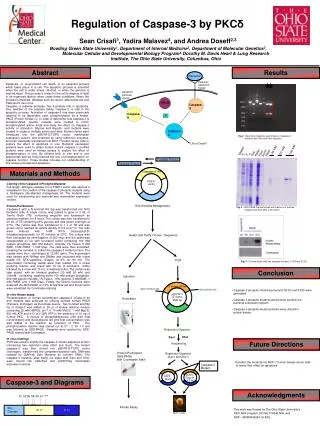
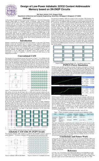
Design of Low-Power Adiabatic 32X32 Content Addressable Memory based on 2N-2N2P Circuits Wei Quan, Advisor: Prof. Xingguo Xiong Department of Electrical and Computer Engineering, University of Bridgeport, Bridgeport, CT 06604 Abstract The structure of adiabatic CAM cell is similar to that of the basic CAM. However, the transistor which previously connects to Gnd is now connected to a clocked power, as shown in Fig. 4. The adiabatic CAM cell consists of a cross-coupled inverter pair (N1, P1, and N2, P2), two pairs of access transistors (NR and NRb, Nw and Nwb), as well as three transistors for the comparison circuits. The two pairs of access transistors are enabled by WWL (write word-line) and RWL (read word-line) for writing and comparison operations, respectively. The power supply of CAM cells is connected to a fixed DC voltage (VDD). The CAM array consists of multiple such cells arrayed horizontally and vertically. The WWL and RWL of a row are connected along with the horizontal axis, while the read bit-lines (RBL and RBL’) and the write bit-lines (search lines) (WBL and WBL’) are connected for all cells in a column[1] .The write operation is similar to the basic CAM. The read word line is enabled row by row. Here, the RW lines do not connect with the comparison part. This can avoid enabling the word line n and comparing the word line n-1 at the same time. At the beginning of the comparison operation, the match line is set in logic low. If it’s a mismatch, the match line will be charged to logic high by the clocked power, and the cell with match data will not affect the match line. The match-lines are driven by the power-clock, thus considerable energy saving can be achieved. Every time after comparing, the voltage of both drain and source of the NMOS transistor connecting to match line will be 0. Hence adiabatic logic can be realized. In this poster, the implementation of a low power adiabatic 32×32 Content Addressable Memory (CAM) based on 2N-2N2P circuits is proposed. CAM memory includes comparison logic with each bit, hence a data value can be broadcasted to all words and compared with the values there. The proposed CAM memory implements adiabatic computing technique in its match-lines to achieve effective energy savings. Furthermore, a novel 2N-2N2P circuit is utilized to recover the charge of node capacitances on address decoders, bit-lines and word-lines. Such architecture leads to significant power reduction in its comparison operations due to the fact that the energy transferred to the capacitance buses can be recovered from adiabatic computing. In order to compare the effectiveness of the power savings, a 32×32 CAM based on conventional CMOS logic is also implemented. Both circuits are designed and simulated in PSPICE. PSPICE power simulation is used to extract the power consumption of both circuits for the same giving input pattern sequence. Simulation results demonstrate effective power savings of the adiabatic CAM based on 2N-2N2P circuits. Such memory architecture can be a good choice for low power memory design. Introduction Adiabatic computing has attracted more and more attention in low power VLSI design. Adiabatic circuits use "reversible logic" to conserve energy. Traditional CMOS circuits dissipate energy during switching. However, adiabatic circuits attempt to conserve charge by two ways: a). never turn on a transistor when there is a voltage potential between source and drain, b). never turn off a transistor when current is flowing through it. In [1], a low power adiabatic CAM based on 2N-2N2P circuits is reported. In this project, we implemented a 32×32 CAM based on 2N-2N2P circuits, and simulated its power consumption. In order for comparison, a 32×32 conventional CAM memory is also designed and simulated. Conventional CAM The structure of a conventional memory cell is shown in Figure 1. It is a RAM cell with three additional transistors for comparison operation. Figure 2 shows a block of 8×8 cell array, and Figure 3 shows the block diagram of the whole 32×32 conventional CAM. The search lines are distributed vertically and bring the search bit to the storage cell. The match lines run horizontally to show whether the search bit matches the word stored in the memory array. In the PSPICE simulation, the word lines are enabled row by row. In the same time, the search line will give the initial storage voltage to all the memory cells. In addition, a DC voltage source is used to pre-charge all the match lines with a NMOS transistor to control the pre-charge time. Figure 6. PSPICE schematic design of 32×32 adiabatic memory array PSPICE Power Simulation PSPICE power simulation is used to simulate the power consumption of both the conventional CAM and adiabatic CAM with same data patterns after same reading and writing operations. The storage-cell array is identical for both CAM designs. The conventional CAM employs CMOS logic circuits to drive all address decoders, bit-lines and word-lines. To reduce simulation time, PSPICE power simulation was done for a subset of the memory that includes a 2x2 cell array block, which is a partial block of the memory array shown in Figure 2 and 4. Figure 7. PSPICE power simulation for conventional CAM Figure 1. The conventional CAM cell circuit Figure 2. A block of 8×8 cell array After writing all the bits into the target cells, a CAM search operation begins with pre-charging all match-lines to 5V. Then, the search line drivers broadcast the search data into the search lines. Each CAM cell compares its stored bit with the bit on its corresponding search line. The cells with matching data do not affect the states on match-lines, but the cells with a mismatch data will pull down the corresponding match-lines. As a result, the match-lines are pulled down for any word that has at least one mismatch in that row. The match-lines without any mismatch will keep its initial logic-high state (5V). As we know, the comparison operations are the major source of power dissipation. Typically, a CAM has only a small number of word matches, and most of them mismatch. Since mismatches are dominative, most match-lines are always both pre-charged and evaluated during every cycle. Further, the search-lines and word-lines are another large source of power dissipation in CAM, because they have high switching activity and contain large node capacitances. This leads to high power consumption on the match-lines, search-lines and word-lines. Figure 8. PSPICE power simulation for adiabatic CAM PSPICE power simulation results for both conventional and adiabatic CAM cells are shown in Figure 7 and 8. The clock period is set as 300ns,and totally 8 patterns are simulated. Conventional CAM and adiabatic CAM have the same patterns and both of them show correct waveforms at output ML in PSPICE simulation. As we can see from the power curves, the average power consumption of the conventional CAM without adiabatic cell is Pavg_original(T) = 5.5340×10⁻³W. For the circuit with adiabatic cell, the average power consumption for the same given pattern sequence is Pavg_adiabatic(T) =0.678795×10⁻³ W, as shown in Table 1. As a result, for the given input sequence, the percentage power savings of the adiabatic CAM compared to conventional CMOS CAM is: Psave=[(5.534mW-0.678795mW)/5.534mW]×100%=87.73% Table 1. Power comparison between conventional and adiabatic CAMs This result demonstrates a significant power savings of 87.73% for the circuit with adiabatic cell. This power saving is mainly due to following 2 reasons. First, the writing operation and comparison operations are divided into 2 parts of circuit. While the storage bits are written into the array row by row, in adiabatic circuit, the writing operation for line N will not cause the comparison of line N-1 in adiabatic circuit. Second, a clock voltage is used to charge the match-line instead of pulling it down when the storage bit is a mismatch. This means that we do not need to pre-charge all the march-lines in every cycle. Every time when the NMOS transistor connected to match line is turned off, there is no voltage difference between its source and drain. Hence the power consumption is reduced. Figure 3. PSPICE schematic design of 32×32 conventional memory array Adiabatic CAM with 2N-2N2P Circuits The proposed adiabatic CAM consists of a CAM-cell with 2N-2N2P circuits to reduce its power dissipation. The states in adiabatic CAM are opposite to the conventional CAM. Conclusions and Future Work In this poster, the design and simulation of a 32×32 low power adiabatic CAM using 2N-2N2P circuits is proposed. Simulation results demonstrate an effective power saving of 87.73% in adiabatic CAM using 2N-2N2P circuits compared to conventional design. In the future work, we will aim at further reducing the power consumption of the CAM memory. For example, it is observed that generally mismatching is dominative in memory search operation. Thus if we use logic “0” (instead of “1”) to represent the mismatch on ML, the power consumption may be further reduced. Furthermore, we will extend this adiabatic computing concepts to other combinational circuits (e.g. full adder, multiplier, ALU) as well. Reference [1] Y. Wu, J. Hu, "Low-Power Content Addressable Memory Using 2N-2N2P Circuits", Proc. of Int. Conf. on Communications, Circuits and Systems, pp. 2657 – 2661, 2006. [2] Y. Moon, and D. K. Jeong, "A 32 x 32-b adiabatic register file with supply clock generator", IEEE Journal of Solid-State Circuits, Vol.33, No. 5, pp. 696 -701, 1998. Figure 4. Adiabatic CAM cell (2N-2N2P) Figure 5. A block of 8×8 adiabatic cell array