Download
1 / 5
50 likes | 64 Views
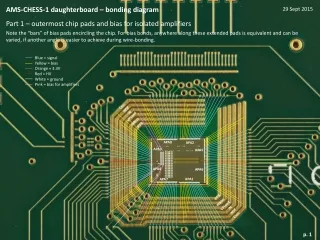
AMS-CHESS-1 daughterboard – bonding diagram Part 1 – outermost chip pads and bias for isolated amplifiers

E N D
AMS-CHESS-1 daughterboard – bonding diagram Part 1 – outermost chip pads and bias for isolated amplifiers Note the “bars” of bias pads encircling the chip. For bias bonds, anywhere along these extended pads is equivalent and can be varied, if another angle is easier to achieve during wire-bonding. 29 Sept 2015 Blue = signal Yellow = bias Orange = 3.3V Red = HV White = ground Pink = bias for amplifiers Casc iNSF iN VPLoad iNBias iPFB APA8 APA2 APA3 APA5 APA4 APA6 APA1 APA7 iPFB iNBias VPLoad iN iNSF Casc
AMS-CHESS-1 daughterboard – bonding diagram Part 2 – inner throw for isolated amplifiers (chip pads 12 to 18, Out1 to Out7) + bonds for Large Passive Array This is a layer arcing over the bonds for active pixel arrays APA3, APA8 and APA2. Blue = signal Yellow = bias Orange = 3.3V Red = HV White = ground Bonds for large passive array Casc iNSF iN VPLoad iNBias iPFB APA8 APA2 APA3 APA5 APA4 APA6 APA1 APA7 iPFB iNBias VPLoad iN iNSF Casc
AMS-CHESS-1 daughterboard – bonding diagram Part 3 – outer throw for isolated amplifiers (chip pads 2 to 8, In1 to In7) This is a layer arcing over the inner throw for the isolated amplifiers, or interspersed with the inner throw. Bonds anywhere along the long vertical input ‘bar’ pad are equivalent. Blue = signal Yellow = bias Orange = 3.3V Red = HV White = ground Casc iNSF iN VPLoad iNBias iPFB APA8 APA2 APA3 APA5 APA4 APA6 APA1 APA7 iPFB iNBias VPLoad iN iNSF Casc
AMS-CHESS-1 daughterboard – bonding diagram Part 4 – bonds for capacitors and high voltage Capacitors should be glued with non-conductive glue Blue = signal Yellow = bias Orange = 3.3V Red = HV White = ground VDD3V3 If supplying HV via central Lemo hole, bond these pads multiple times If supplying HV via edge connector, bond these pads multiple times VDD3V3 iNSF iN iPFB
Capacitor specifications: Manufacturer: Ipdia Part number: EMSC 42F.610 (935.121.42F.610) Value: 100nF Size: 0404 Height: 100µm Notes about capacitors Capacitors should be glued with non-conductive glue. Pins 1 & 2 are tied together; pins 3 & 4 are tied together. Orientation for C1, C4, C5 and C6: Orientation for C3: Label expected to be E6101 on all capacitors This connecting bar is probably the best feature for orienting the capacitors. C1 = VDD3V3 to GND C4 = iN to GND C3 = VDD3V3 to GND C5 = iPFB to VDD3V3 Note, there is no C2 (by oversight) C6 = iNSF to GND