Download
1 / 18
180 likes | 311 Views
The DVP-525 project proposes an innovative 16-bit Delta-Sigma Analog-to-Digital Conversion chip aimed at enhancing voice quality in applications such as VoIP, digital telephony, and digital hearing aids. The design incorporates advanced oversampling techniques and noise shaping to achieve exceptional signal-to-noise ratios. Key features include a Sinc3 filter for decimation and a peak input indicator for audio level monitoring. Additionally, the architecture is optimized for efficient digital logic and stability, making it suitable for market-ready voice solutions.

E N D
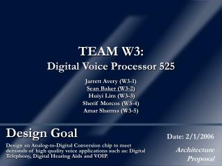
TEAM W3:Digital Voice Processor 525 Jarrett Avery (W3-1) Sean Baker (W3-2) Huiyi Lim (W3-3) Sherif Morcos (W3-4) Amar Sharma (W3-5) Design Goal Date: 2/1/2006 Architecture Proposal Design an Analog-to-Digital Conversion chip to meet demands of high quality voice applications such as: Digital Telephony, Digital Hearing Aids and VOIP.
Status • Design Proposal • Project chosen: 16 bit Delta-Sigma ADC • Basic specs defined • Architecture • Matlab Simulated • Behavioral Verilog – Done, but not simulated • Schematic • Floorplanning • Layout • Simulation / Verification
In Case You Forgot…(A Summary of Last Week) • Applications of the DVP-525 • VoIP, Digital Telephony, Encrypted Communications • Digital Hearing Aids • How the DVP-525 works: • Uses Delta-Sigma modulation of input signal and decimation to convert an analog signal into 16 bit binary numbers
Algorithm Detail Lowpass Filter Analog to Digital Conversion (Delta-Sigma Modulator) Decimation (Sinc Filter, Downsample) Analog Input Digital Output Measure Peak Amplitude (Peak Input Indicator) Digital Peak Indicator
Hardware That Makes it Happen(Modulator) Integrators Comparator
Algorithm Detail Lowpass Filter Analog to Digital Conversion (Delta-Sigma Modulator) Decimation (Sinc Filter, Downsample) Analog Input Digital Output Measure Peak Amplitude (Peak Input Indicator) Digital Peak Indicator
Hardware That Makes it Happen(Decimator) These accumulators and registers are clocked at the sampling frequency: (Nyquist Clock * 256) These differencers and registers are clocked at the Nyquist rate
Algorithm Detail Lowpass Filter Analog to Digital Conversion (Delta-Sigma Modulator) Decimation (Sinc Filter, Downsample) Analog Input Digital Output Measure Peak Amplitude (Peak Input Indicator) Digital Peak Indicator
Important Concepts for Delta-Sigma ADCs • Oversampling • Nyquist Frequency – minimum frequency for reconstruction of signal • OSR – Oversampling Ratio, fS / fN • Oversampling spreads out noise spectrum • For 2nd order modulator, signal to noise ratio (SNR) increases by 15dB (32x higher) for each doubling of OSR
Effects of Oversampling amplitude amplitude Band of Interest Band of Interest Diminished Noise Noise freq freq fS = fN fS = fN * OSR
More Important Concepts • Noise Shaping • Integrator in feed-forward path and DAC in feedback path pushes noise out of signal bandwidth
Transistor Estimate • Analog • 3 x Analog Op Amps, 3 x 24 = 72 • Capacitive Resistive Elements • Digital • 8 x 18 bit registers, 8 x 250 = 2000 • 6 x 18 bit adders, 6 x 500 = 3000 • 2 x 18 bit comparators, 2 x 800 = 1600 • 1 x 24 bit counter, 1 x 1000 = 1000 • 1 x 24 bit comparator, 1 x 1000 = 1000 • 4 x 18 bit muxes, 4 x 150 = 600 • Misc logic = 200 • Total Transistors = 9,472
Simulation • First modeled the modulator in the time domain, and fed it a simple sine wave input:
Simulation (cont’d) • Then fed the bitstream created by the modulator into the decimator:
Design Decisions • Chose 2nd order Delta-Sigma Modulator • Eases speed requirements (lower OSR) • Makes digital logic simpler • Stability issues won’t be crippling • Chose Sinc3 filter for decimation • For Lth order modulator, need L+1 order Sinc filter • Not a perfect LPF, but pretty good & economical • Bandwidth of interest – 20 Hz to 10 KHz • Focuses on voice applications, but doesn’t limit product • Decided on OSR of 256 • Gives 16 effective bits of resolution • Makes sampling frequency 256*(10 KHz * 2) = 5.12 MHz • Optional digital function: Peak Input Indicator (PII) • Holds value of highest and lowest amplitude (refreshes every few seconds) • Could be used to prevent blowing out speakers, etc.
Problems and Questions • Is the decimation filter enough for the digital section of the project? • Use higher order sinc filter, faster adders? • Include PII? • Input 2 clock signals to the decimator, or input 1 clock and generate the 2nd from the 1st? • Analog Issues • How fast do the op-amps need to run (settling time, stability, etc.) • What gain is required of op-amps? • Active or passive Butterworth filter for the input? • Input voltage levels? Pre-amplification?
Results • More comfortable with overall design • A lot of this is new to us… • We have a marketable product • Ready to move forward with design • Gate level verilog for the digital parts • Topology, gate sizing, RLC selection for analog parts