ALTERA Quartus II Software
ALTERA Quartus II Software. 목 차. 프로젝트 생성 VHDL 컴파일 시뮬레이션 디바이스와 핀 할당 FPGA 에 다운로드 계층적 프로젝트. 프로젝트 생성 ( 새로운 프로젝트 생성 ). File New Project Wizard Project name 과 top-level design entry name 을 일치. 프로젝트 생성 ( 새로운 프로젝트 생성 ). Project 에 포함시킬 design file 을 선택 없으면 Next> 를 클릭.

ALTERA Quartus II Software
E N D
Presentation Transcript
목 차 • 프로젝트 생성 • VHDL 컴파일 • 시뮬레이션 • 디바이스와 핀 할당 • FPGA에 다운로드 • 계층적 프로젝트
프로젝트 생성(새로운 프로젝트 생성) • File New Project Wizard • Project name과 top-level design entry name을 일치.
프로젝트 생성(새로운 프로젝트 생성) • Project에 포함시킬 design file을 선택 • 없으면 Next>를 클릭
프로젝트 생성(새로운 프로젝트 생성) • Device 선택 • Cyclone EP1C4F324C8을 선택
프로젝트 생성(새로운 프로젝트 생성) • 함께 사용할 EDA tool을 선택 • 없으면 Next>를 클릭
프로젝트 생성(새로운 프로젝트 생성) • Finish 클릭으로 project 생성 종료
프로젝트 생성(새로운 프로젝트 생성) • 새로운 project가 생성된 것을 확인
프로젝트 생성(새로운 프로젝트 생성) • File New VHDL file 선택하여 VHDL 프로그래밍
프로젝트 생성(새로운 프로젝트 생성) • File Save As 에서 vhd 확장자로 새로운 파일을 저장
Project의 생성(기존 project open) • File Open Project 선택
Project의 생성(기존 project open) • Project가 open된 것을 확인
VHDL 컴파일 • Processing Start Compilation 또는 Compiler Tool을 클릭 • Start Compilation 단축 아이콘 “►”을 직접 클릭
시뮬레이션 • File New를 클릭한 후 Vector Waveform File을 선택
시뮬레이션 • File Save As를 클릭하여 *.vwf 파일로 저장
시뮬레이션 • Name위 마우스 우측버튼 클릭 후 Insert Insert Node or Bus 선택
시뮬레이션 • Node Finder를클릭한 후 Filter:에서 Pins:all을 선택한 후 List를 클릭하면 입출력 단자의 이름이 나타남
시뮬레이션 • Nodes Found에서 모든 노드를 선택한 후 Selected Nodes로 모두 이동
시뮬레이션 • 신호의 범위를 정한 후 좌측 신호 레벨을 클릭하여 입력 신호 값을 결정
시뮬레이션 • Processing Start Simulation 또는 Simulation Tool을 클릭 • 단축 아이콘 을 직접 클릭
시뮬레이션 • Simulation Tool에서 버튼 클릭 또는 • Overwrite simulation input …을 체크하고 open을 클릭
시뮬레이션 • 시뮬레이션 결과를 확인
시뮬레이션 • Simulation 시간 조정 • Edit End Time에서 end time을 설정
디바이스와 핀 할당 • Assignment Device 메뉴에서 Cyclone EP1C4F324C8을 선택
디바이스와 핀 할당 • Device and Pin Options : Active Serial로 선택 • Use configuration device 체크 EPCS1 선택
디바이스와 핀 할당 • Assignment Pin을 클릭하고 핀 번호 할당
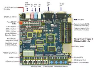
디바이스와 핀 할당 • DigComV32의 입출력 장치
디바이스와 핀 할당 • 키보드(KEY 0 ~ KEY F) • 슬라이드 스위치(SW24 ~ SW31) • Reset, Oscillator • 3단 슬라이드 스위치(SW3) • LED(D16 ~ D18) • LED(D1 ~ D8) • LED(D9 ~ D15)
디바이스와 핀 할당 • 7-Segment
FPGA에 다운로드하기 • Tools Programmer 또는 Programmer 단축아이콘 실행
FPGA에 다운로드하기 • Hardware Setup Add Hardware 클릭 • Hardware Type : ByteBlasterII, Port : LPT1
FPGA에 다운로드하기 • Available hardware items : ByteblasterII • Currently Selected hardware : ByteblasterII
FPGA에 다운로드하기 • Mode Active Serial 선택
FPGA에 다운로드하기 • Add file에서 다운로드할 pof 파일 선택 • Program/Configure 체크
FPGA에 다운로드하기 • Start 버튼을 클릭하면 Progress bar에서 다운로드되는 것을 확인
계층적 프로젝트 • 기능단위 블록으로 설계를 한 후 상위 계층에서 Graphic design • 예) 4x1 멀티플렉서와 Altera D Flip-Flop를 이용한 설계 • 새로운 폴더에 mux41 프로젝트 생성, mux41.vhd 설계
계층적 프로젝트 • File Create/Update Create Symbol File for Current File 실행 BSF파일
계층적 프로젝트 • Top level project를 같은 디렉토리에 생성
계층적 프로젝트 • File New Block Diagram/Schematic File 선택
계층적 프로젝트 • 마우스 더블 클릭, Project mux41 심볼 선택
계층적 프로젝트 • 심볼을 화면에 배치
계층적 프로젝트 • 마우스 더블 클릭, libraries primitives storage dff 선택
계층적 프로젝트 • Block Design/Schematic 설계 완료후 *.bdf로 저장
계층적 프로젝트 • 컴파일 성공