Designing Custom Single-Purpose Processors: RT-Level Techniques and Optimization Strategies
In this week's Digital II course, we explore RT-level custom single-purpose processor design. Topics include combinational and sequential logic, introduction to custom processor design, and detailed analysis of the design of an RT-level single-purpose processor that converts two 4-bit inputs into one 8-bit output. We discuss the importance of Finite State Machine Data Paths (FSMDs) and optimization strategies for processor design. Additionally, we’ll examine the significant factors for improving performance and reducing complexity in custom designs, and complete design exercises focused on real-world applications.

Designing Custom Single-Purpose Processors: RT-Level Techniques and Optimization Strategies
E N D
Presentation Transcript
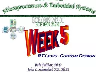
DIGITAL II Microprocessors & Embedded Systems ECE 0909.242.01 Week 5 RT-Level Custom Design Robi Polikar, Ph.D. John L. Schmalzel, P.E., Ph.D.
This Week in DIG II Chapter 2: Custom single-purpose processors • Introduction • Combinational logic • Sequential logic • Custom single-purpose processor design • Review • RT-level custom single-purpose processor design • Tomorrow in the lab…. • Continue working on this week’s assignment • Add computational functionality • Surreal moments with Dr. P.
RT-level custom single-purpose processor design clock Sender Bridge A single-purpose processor that converts two 4-bit inputs, arriving one at a time over data_in along with a rdy_in pulse, into one 8-bit output on data_out along with a rdy_out pulse. Receiver 4 8 data_in(4) data_out(8) rdy_in rdy_out • We often start with a state machine • Rather than algorithm • Cycle timing often too central to functionality • Programming languages don’t support cycle-by-cycle timing • FSMDs make cycle-by-cycle timing explicit • Example • Bus bridge that converts 4-bit bus to 8-bit bus • Start with FSMD • Known as register-transfer (RT) level • Exercise: complete the design Problem Specification rdy_in=0 rdy_in=1 rdy_in=1 WaitFirst4 RecFirst4Start data(3..0)=data_in RecFirst4End rdy_in=0 rdy_in=0 rdy_in=1 rdy_in=1 WaitSecond4 RecSecond4Start data(7..4)=data_in RecSecond4End FSMD rdy_in=0 Send8Start data_out=data rdy_out=1 Send8End rdy_out=0
RT-level custom single-purpose processor design (cont’) rdy_in=0 rdy_in=1 rdy_in=1 WaitFirst4 RecFirst4Start data_lo_ld=1 RecFirst4End rdy_in=0 rdy_in=0 rdy_in=1 rdy_in=1 WaitSecond4 RecSecond4Start data_hi_ld=1 RecSecond4End Send8Start data_out_ld=1 rdy_out=1 Send8End rdy_out=0 Bridge (a) Controller Create the data path using the 4-step process as before, and convert FSMD to FSM (controller) rdy_in rdy_out clk data_in(4) data_out data_hi data_lo to all registers data_lo_ld data_hi_ld data_out_ld data_out (b) Datapath
A Few Points to Remember • We have seen two custom single purpose processor design procedure, one that starts with a software program, the other directly at the FSMD level. • Which one to use when? • Use the former program based method, whenever the problem requires for algorithm implementation, heavy math, etc. • Use the latter method, whenever the problem is mostly a control application (like our bridge example). • Starting at FSMD level is also known as Register-Transfer (RT) level design, since an FSMD describes which registers have their data transferred to which other registers at each state.
Optimizing single-purpose processors • In GCD example, we ignored several simplification opportunities : • The FSM had several states did not do anything • Datapath had two adders, where in fact, one may be sufficient • Etc. • In a typical real custom design task, we typically wish to optimize every possible parameter / procedure. • Optimization is the task of making design metric values the best possible • Optimization opportunities • original program • FSMD • datapath • FSM
Optimizing the original program • Analyze program attributes and look for areas of possible improvement • number of computations • size of variable • time and space complexity • operations used • multiplication and division very expensive
Optimizing the original program (cont’) optimized program original program 0: int x, y, r; 1: while (1) { 2: while (!go_i); // x must be the larger number 3: if (x_i >= y_i) { 4: x=x_i; 5: y=y_i; } 6: else { 7: x=y_i; 8: y=x_i; } 9: while (y != 0) { ??????? } 13: d_o = x; } 0: int x, y; 1: while (1) { 2: while (!go_i); 3: x = x_i; 4: y = y_i; 5: while (x != y) { 6: if (x < y) 7: y = y - x; else 8: x = x - y; } 9: d_o = x; } GCD(42, 8) - 9 iterations to complete the loop x and y values evaluated as follows : (42, 8), (43, 8), (26,8), (18,8), (10, 8), (2,8), (2,6), (2,4), (2,2).
Optimizing the FSMD • Areas of possible improvements • merge states • states with constants on transitions can be eliminated, transition taken is already known • states with independent operations can be merged • separate states • states which require complex operations (a*b*c*d) can be broken into smaller states to reduce hardware size • t1=b*c, t2=d*e, a=t1*t2 requires only one MUX (as opposed to three) • Scheduling: the task of assigning operations from the original problem to states in an FSMD • Beware: Note that the optimized process will take fewer clock cycles. This may not be acceptable for certain application that are highly clock dependent!
Optimizing the FSMD (cont.) int x, y; !1 1: int x, y; 1 !(!go_i) 2: 2: go_i !go_i !go_i x = x_i y = y_i 2-J: 3: x = x_i 3: 5: 4: y = y_i x<y x>y y = y -x 8: x = x - y 7: !(x!=y) 5: x!=y 9: d_o = x 6: x<y !(x<y) y = y -x x = x - y 8: 7: 6-J: 5-J: d_o = x 9: 1-J: original FSMD optimized FSMD Beware: Avoid the common mistake of assuming that a variable assigned in a state can have the newly assigned value on an outgoing arc of that state
Optimizing the datapath • Sharing of functional units • one-to-one mapping, as done previously (two separate subtractors), may not necessary • if same operation occurs in different states, they can share a single functional unit (use single subtractor, with a MUX whose control bit chooses the inputs as (xand y)or (y and x). • Multi-functional units • ALUs support a variety of operations, it can be shared among operations occurring in different states
Optimizing the FSM • State encoding • task of assigning a unique bit pattern to each state in an FSM • size of state register and combinational logic vary • can be treated as an ordering problem • State minimization • task of merging equivalent states into a single state • state equivalent if for all possible input combinations the two states generate the same outputs and transitions to the next same state • Note that the state merging done in the previous example is NOT state minimization, because we changed the timing of the circuit. By the time we arrive at FSM, the timing of the output is assumed to be unchangeable !
Summary • Custom single-purpose processors • Straightforward design techniques • Can be built to execute algorithms • Typically start with FSMD • CAD tools can be of great assistance Next time on DIG-II General Purpose Processors: Software