HINS BPM Overview
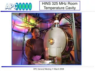
HINS BPM Overview. N. Eddy For Instrumentation Dept. BPM Hardware Overview. 4 button BPM pickup. Down Mix. IF (15). 4. 4. ATT. BPF. LPF. PLL. CTRL. CAN. Cal (xxx). LO (665). beam. CLK (81.25). beam position. I. Digital Receiver (VME). VME µP Motorola 5500.

HINS BPM Overview
E N D
Presentation Transcript
HINS BPM Overview N. Eddy For Instrumentation Dept
BPM Hardware Overview 4 button BPM pickup Down Mix IF (15) 4 4 ATT BPF LPF PLL CTRL CAN Cal (xxx) LO (665) beam CLK (81.25) beam position I Digital Receiver(VME) VME µP Motorola 5500 Timing(VME) TRG Q 325 Trig LAN VME BUS
Analog Signal Processing • 4-ch. Analog downmixer • IN: 650 (2nd harmonic), LO: 665.1, IF: 15.1 MHz • CAN-bus controlled gain, attenuator & cal system • Gain switchable, low-noise, high IP3 input gain stage • Image rejection (SSB) mixer • ~30 dB gain, ultralinear IF stage SSB Mixer Directional Coupler BPF LNA LNA LPF BPF LPF LNA ATT 0° IN OUT 714MHz 15.145 MHz CF: 650MHz BW: 10MHz G: 15 dB NF: 1dB 90° CF: 15.1 MHz BW: 4MHz G: 18 dB BW: 40 MHz BW: 800 MHz G: 14/-2 dB NF: 1dB Cal Tone Signal 0 - 28 dB 4 dB steps 1.6 dB loss LO 665.1 MHz
Generic Digitizer VME bus GATE FPGA Altera Cyclone III VME Drivers TRIGGER External Control TCLK SYNC IN 4x32M DDR2 SDRAM SYNC OUT AC passive ADC JTAG 8 Analog Inputs 4 Channels per Chip EPCS4 Interface ADC Oscillator CLK IN Clock Driver (PLL & DIV) Oscillator CLK OUT 8-Ch,14-bit, 125 MS/s VME Digitizer BLOCK DIAGRAM • 125 MSPS, 500 MHz BW • 4-ch serial ADC chips • 8-ch, AC passive (or DC active) • PLL/VCO CLK distribution • SNR > 72 dB (@50 MHz)
FPGA Block Diagram latch VME NB Sums 50Hz Σ 32 Registers reset VME NB Data 8 ch / NB Filter 1.4kHz output 16 Bits/ch 32 ch / DDR RAM NB Data TBT Data Raw Data ADC Input 14 Bits 69 MHz NB Gate VME TBT Data 16 ch / TBT Filter DDC & average WB Gate(s) VME Raw Data reset latch WB Gate(s) DAQ SM Ch delays (clocks) Gates in Turns VME IRQ Trigger NB Gate
Narrowband Signal Processing NCO (sin, cos) 24 Bits Phase (~1 Hz) Select Significant Bits I • Design footprint for 8 ADC channels • 2 NCOs for beam and cal frequencies -> 16 DDCs • 32 CIC Filters operating at 69 MHz • 5 stage CIC uses 13 k LEs and <1% of RAM • 1 Serial FIR Filter will process all 32 CIC Filter outputs • 76 tap FIR (400 Hz BW, 500 Hz Stop, -120 db stopband) • Decimate by 3 to 1.4 KSPS output CIC 5 Stages R=16485 Bit Shift FIR (76 taps) LPF 500Hz Decimate 3 I 28 pts ave to notch 50 Hz X Q ADC Input 14 Bits 69 MHz DDC Q 16 Bits 16 Bits 1.4 KSPS 24 Bits 4.2 KSPS 20 Bits 4.2 KSPS - Denotes Peak Detectors to optimize scaling
Software Components VME Hardware Motorola 5500 µP Software (VxWorks) Control Control Class ATFBPMCAL Control VME ECAN-2 PMC (1x) Class CALBox Status Status CAN Status Sample Flash WB / NB Bucket Delay 714 Single/Multi-turn VME Timing K-TGF (1x) Turn Data INJ (BIS) Ethernet Class KTGF Control Diag. Mode EPICS IOC Sample Count 2.16 Bucket Delay Class ATFBPM 729 Turn Delay Interrupt CLK (64.9) TRG (Gate) Multi-turn A DDC Configure Control VME Digitizer (12x) Orbit B Class ADC Pos/ Int Data I/Q Data Flash C Diagnostic D Interrupt
Raw Signals from 4/20/11 BPM 1 BPM 3 BPM 2 BPM 1 BPM 3 BPM 2
DDC with Boxcar Filter ~4MHz BW Magn Diff/Sum filtered Sum filtered Magn Diff/Sum filtered Sum filtered
Questions • What information is desired from the BPM? • BW and update rate over the pulse? • Could have WB arrays & pulse averages • Phase measurement (???) • Should produce relative phase along bpms able to detect changes in TOF • Could produce absolute phase if we make a reference bpm from RF… needs some further thought
Summary • Hardware for standard bpms completely installed and working • Firmware/Software for ATF project • Currently only provides 1024 ADC samples • Need to decide exactly what the Firmware should do…