Download

1 / 30
320 likes | 386 Views
Learn about the different types of semiconductor detectors including bolometers, photoconductive detectors, and photovoltaic detectors. Explore the principles, operation, and applications of each detector type in detail. ###

E N D
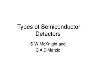
Types of Semiconductor Detectors S W McKnight and C A DiMarzio
Outline • Bolometers • Photoconductive detectors • Photovoltaic detectors
Bolometers Incident Radiation Absorbing film Semiconductor Bolometer Electric leads/ Heat sinks Cryogenically cooled ~ 4.2 K
Semiconductor Bolometer E k Ef Eb Impurity level Binding Energy (Eb) ~ 50 meV
Effect of ΔT on Si Bolometer Conductivity Ambient temperature = 4.2K → kT=0.362 meV Temperature = 4.3K → kT=0.371 meV
Photoconductive Detectors E k Eg
Conductivity Conductivity: σ = n e μ e=electron charge (1.6x10⁻¹⁹ C) =Electron scattering time (average time between scattering events) Mobility:
Photoconductivity Dark current: σd = no e μn + po e μp Photocurrent: σph = Δn e μn + Δp e μp Δn =Δp = photo-induced carrier density (m-3) = Nphη / V Nph = incident photon flux (s-1) η = quantum efficiency = carrier recombination time V = sample volume
Photoconductivity Recombination in n-type material: Steady-state solution: Quantum efficiency: η = (1-R) Pe-h Pe-h = probability of absorption creating electron-hole pair
HgxCd1-xTe Band Gap Eg=-0.302+1.93x+ 5.35x10⁻⁴ T(1-2x) -0.810x2 + 0.823x3 Eg= -0.26eV Eg= 1.6eV HgTe “Zero-gap” (inverted bands) CdTe
Photovoltaic Detectors • P-N junction detector • Incident light creates voltage • Same mechanism as solar cell
P-N Junction E Donor Levels Ef electrons Eg “holes” Ef Acceptor Levels x Doped Semiconductor (p-type) Doped Semiconductor (n-type)
P-N Junction - + E electrons “holes” Ef x
P-N Junction E + - electrons Ef “holes” x Depletion Region
P-N Junction E Ec electrons Ef “holes” Ev - + x Depletion Region
P-N Junction Currents Jdiffusion E Jdrift Ec Junction “built-in” voltage Vo Ef Ev - + x Depletion Region
P-N Junction Currents N-doped material: n≈Nd (# of donors)
P-N Junction Currents (No Bias Voltage) Jdrift = A np = -Jo Jdiffusion = B e-Vo/kT JTotal = -Jo + B e-Vo/kT = 0 (equilibrium) → B= Jo e+Vo/kT
Biased P-N Junction Jdiffusion E Jdrift Ec Vo-Va Va Ef Ev Depletion Region Va x
P-N Junction Currents (Bias Voltage=Va) Jdrift = A np = Jo Jdiffusion = B e-(Vo-Va)/kT JTotal = -Jo + B e-(Vo-Va)/kT B= Jo e+Vo/kT → JTotal = Jo (eVa/kT -1 )
0.09 0.08 0.07 0.06 0.05 Junction Current (Amps) 0.04 0.03 0.02 0.01 0 -0.01 -1 -0.8 -0.6 -0.4 -0.2 0 0.2 0.4 0.6 0.8 1 V (volts) a P-N Junction Current IJunction Io=A Jo = 0.005 A - + VJunction
Photovoltaic Detection Jdiffusion E Jdrift Ec Junction “built-in” voltage Vo Ef Ev - + Depletion Region x
Photovoltaic Detection • Absorption in depletion region creates electrons/hole pairs • Built in electric field accelerates electrons and holes toward neutral region • Photocurrent adds Iph= ηe Nph to drift current
P-N Junction Photocurrent 0.06 Io=A Jo = 0.005 A 0.04 Iph=A Jph = 0.02 A Junction Current (Amps) 0.02 0 -0.02 -1 -0.8 -0.6 -0.4 -0.2 0 0.2 0.4 0.6 0.8 1 V (volts) a
Photovoltaic Sensing Circuit + Vph -
Photoconductive Sensing Circuit Iph - + Vd
Photoconductive Detection E Jdrift Ec Vo+ Vd Ev Ef - + Depletion Region x
Avalanche Photodetection E Jdrift Ec Vo+ Vd Ev Ef Depletion Region x
Avalanche Photodiode • Large reverse bias on junction • Photoelectrons create electron/hole pairs in depletion region • Electron and holes can create more electron/hole pairs • Device has gain (like PMT)