Download

1 / 98
980 likes | 1.16k Views
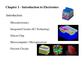
Chapter 1 - Introduction to Electronics. Introduction Microelectronics Integrated Circuits (IC) Technology Silicon Chip Microcomputer / Microprocessor Discrete Circuits. Signals Signal Processing Transducers. http://www.eas.asu.edu/~midle/jdsp/jdsp.html. Signals Voltage Sources

E N D
Chapter 1 - Introduction to Electronics • Introduction • Microelectronics • Integrated Circuits (IC) Technology • Silicon Chip • Microcomputer / Microprocessor • Discrete Circuits
Signals • Signal Processing • Transducers http://www.eas.asu.edu/~midle/jdsp/jdsp.html
Signals • Voltage Sources • Current Sources • Thevenin & Norton • http://www.clarkson.edu/%7Esvoboda/eta/ClickDevice/refdir.html • http://www.clarkson.edu/%7Esvoboda/eta/Circuit_Design_Lab/circuit_design_lab.html • http://www.clarkson.edu/%7Esvoboda/eta/CircuitElements/vcvs.html
Figure 1.1 Two alternative representations of a signal source: (a) the Thévenin form, and (b) the Norton form.
Figure 1.3 Sine-wave voltage signal of amplitude Va and frequency f = 1/T Hz. The angular frequency v = 2pf rad/s.
Signals • Voltage Sources • Current Sources
Signals • Voltage Sources • Current Sources http://www.clarkson.edu/~svoboda/eta/ClickDevice/super.html http://javalab.uoregon.edu/dcaley/circuit/Circuit_plugin.html
Frequency Spectrum of Signals • Fourier Series • Fourier Transform • Fundamental and Harmonics • http://www.educatorscorner.com/experiments/spectral/SpecAn3.shtml frequency time
Figure 1.5 The frequency spectrum (also known as the line spectrum) of the periodic square wave of Fig. 1.4.
Figure 1.6 The frequency spectrum of an arbitrary waveform such as that in Fig. 1.2.
Figure 1.7 Sampling the continuous-time analog signal in (a) results in the discrete-time signal in (b).
Frequency Spectrum of Signals • Fourier Series http://www.jhu.edu/%7Esignals/fourier2/index.html
Frequency Spectrum of Signals • Fourier Series
Frequency Spectrum of Signals • Fourier Series
Frequency Spectrum of Signals • Fourier Series
Frequency Spectrum of Signals • Fourier Series
Frequency Spectrum of Signals • Fourier Series
Frequency Spectrum of Signals http://www.jhu.edu/%7Esignals/fourier2/index.html http://www.jhu.edu/%7Esignals/listen/music1.html http://www.jhu.edu/%7Esignals/phasorlecture2/indexphasorlect2.htm
Figure 1.8 Variation of a particular binary digital signal with time.
Figure 1.9 Block-diagram representation of the analog-to-digital converter (ADC).
Analog and Digital Signals • Sampling Rate http://www.jhu.edu/%7Esignals/sampling/index.html • Binary number system • http://scholar.hw.ac.uk/site/computing/activity11.asp • Analog-to-Digital Converter • http://www.astro-med.com/knowledge/adc.html • http://www.maxim-ic.com/design_guides/English/AD_CONVERTERS_21.pdf • Digital-to-Analog Converter • http://www.maxim-ic.com/ADCDACRef.cfm
Figure 1.10 (a) Circuit symbol for amplifier. (b) An amplifier with a common terminal (ground) between the input and output ports.
Figure 1.11 (a) A voltage amplifier fed with a signal vI(t) and connected to a load resistance RL. (b) Transfer characteristic of a linear voltage amplifier with voltage gain Av.
Figure 1.12 An amplifier that requires two dc supplies (shown as batteries) for operation.
Figure 1.13 An amplifier transfer characteristic that is linear except for output saturation.
Figure 1.14 (a) An amplifier transfer characteristic that shows considerable nonlinearity. (b) To obtain linear operation the amplifier is biased as shown, and the signal amplitude is kept small. Observe that this amplifier is operated from a single power supply, VDD.
Figure 1.15 A sketch of the transfer characteristic of the amplifier of Example 1.2. Note that this amplifier is inverting (i.e., with a gain that is negative).
Figure 1.17 (a) Circuit model for the voltage amplifier. (b) The voltage amplifier with input signal source and load.
Figure 1.19 (a) Small-signal circuit model for a bipolar junction transistor (BJT). (b) The BJT connected as an amplifier with the emitter as a common terminal between input and output (called a common-emitter amplifier). (c) An alternative small-signal circuit model for the BJT.
Figure 1.20 Measuring the frequency response of a linear amplifier. At the test frequency v, the amplifier gain is characterized by its magnitude (Vo/Vi) and phase f.
Figure 1.21 Typical magnitude response of an amplifier. |T(v)| is the magnitude of the amplifier transfer function—that is, the ratio of the output Vo(v) to the input Vi(v).
Figure 1.22 Two examples of STC networks: (a) a low-pass network and (b) a high-pass network.
Figure 1.23 (a) Magnitude and (b) phase response of STC networks of the low-pass type.
Figure 1.24 (a) Magnitude and (b) phase response of STC networks of the high-pass type.
Figure 1.26 Frequency response for (a) a capacitively coupled amplifier, (b) a direct-coupled amplifier, and (c) a tuned or bandpass amplifier.
Figure 1.28 A logic inverter operating from a dc supply VDD.
Figure 1.29 Voltage transfer characteristic of an inverter. The VTC is approximated by three straightline segments. Note the four parameters of the VTC (VOH, VOL, VIL, and VIH) and their use in determining the noise margins (NMH and NML).
Figure 1.31 (a) The simplest implementation of a logic inverter using a voltage-controlled switch; (b) equivalent circuit when vIis low; and (c) equivalent circuit when vIis high. Note that the switch is assumed to close when vIis high.
Figure 1.32 A more elaborate implementation of the logic inverter utilizing two complementary switches. This is the basis of the CMOS inverter studied in Section 4.10.
Figure 1.33 Another inverter implementation utilizing a double-throw switch to steer the constant current IEE to RC1 (when vI is high) or RC2 (when vI is low). This is the basis of the emitter-coupled logic (ECL) studied in Chapters 7 and 11.