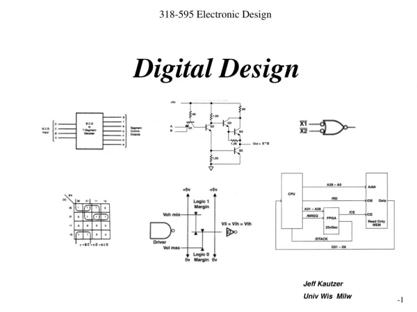
Digital Design
Digital Design. Jeff Kautzer Univ Wis Milw. Basic Combinatorial Timing Parameters. TpHL(TpLH): Propagation Delay from High to Low (Low to High) Logic Level Usually measured between the 10% and 90% total voltage transition points.

Digital Design
E N D
Presentation Transcript
Digital Design Jeff Kautzer Univ Wis Milw
Basic Combinatorial Timing Parameters • TpHL(TpLH): Propagation Delay from High to Low (Low to High) Logic Level Usually measured between the 10% and 90% total voltage transition points. • Tpd or Tp: Propagation Delay usually stated as worst case of TpHL and TpLH. • Tott or Tout: Output Transition Time. For many families (HC, HCT, etc), gate delays are stated with separate specifications for logical output value generation (Tpd) plus physical output voltage transition (Tott). Need to sum these for total prop delay !! • TpzH(TpzL): Propagation Delay from High Impedance to High (Low) Logic Level • TpHz(TpLz): Propagation Delay from High (Low) Logic Level to High Impedance
Basic Sequential Timing Parameters • Tsu: Setup Time, Data must be stable this min time prior to CLK edge • Th: Hold Time, Data must remain stable this min time after CLK edge • Td: CLK to Q or Output Delay, Time for Data Propagation to Q • Tset/Treset: Control Input to Output Change delay • Tw: Min Control Input Width (active low) • Tclk: Min Logic 1 (high) + Min Logic 0 (low) time for CLK signal. May be stated separately or as Max Frequency (Fmax). • Note: Tclk – (Tsu + Th) = Worst Case usable time to change data.
Missing Tsu or Th ….. Possible Results • FF latches the data normally as if Tsu and Th were satisfied • FF misses the intended data but clocks data at next opportunity • FF misses the intended data completely, lost • FF latches the correct data but with extended Td • FF latches the correct data but exhibits many output transitions • FF misses the intended data and exhibits many output transitions • FF misses the data and causes other spurious affects Metastable Behaviour
Characterizing Metastable Likelyhood Fd can be estimated using a worst case assumption based on clock frequency • To and t: Technology (family) specific, usually published in a separate metastability characterization report from the Mfg. • Tw: Walkout time allowable within a given application (1/Fc – Tsu – Th) in many cases
Examples: To & t, Metastability Constants Worst Case Metastability Analysis Clearly this device is not well suited for the intended application ! Metastability MTBFs Need to Be >> 100 years
Improvement Using Better (faster) Device Using Metastable hardened Device Enormous difference in Metastability Performance of Device Technologies
Synchronization also used to improve “System” Immunity to Metastability Same Example Using Multistage Synchronization Synchronization Causes System Response Time Penalty
Using Timing Parameters, Timing Analysis Simple Data Transfer Example: 10Mhz CPU Memory Read Cycle • Timing Diagram notation uses binary signals (CLK, Controls) and bussed signals (Address and Data) • CPU Generates System Timing relative to a master CLK. Sends out Address and Control Signals, Expects Data in T3 • Basic Memory Read Cycle is 3 CLKs long but can be extended using the DTACK (Wait State) signal • CPU Samples DTACK in T2, if non-active, T2 is repeated (Wait State); if active, T2 ends followed by T3 • CPU Expects Data at midpoint of T3, Note Data Setup Time and Data Hold Time Requirements • Timing Analysis Determines if Target Memory Device is Fast Enough or if it requires Wait States
Timing Analysis Using the “Target” device as viewpoint Read-Only-Memory is Target Device Target Device Timing Parameters • Target has 3 basic input signals • Address: Specifies 1 storage location in device to be read • CE (active low): Disables entire device including selector system and output driver • OE (active low): Disable output driver only
Timing Analysis… To Get the Data • Possible Improvements: • Use Faster FPGA with lower Tpd • Exercise 1 wait state using DTACK
Timing Analysis… To Finish the Cycle Can Memory disable output drive in time?
General State Machine Architecture Inputs Output Decoder Logic Next State Comb Logic State Variables (FF) Array Possible Outputs Outputs Present State Info CLK Mealy Architecture Requires Output Decoder Logic Block
Review: State Machine Design Typical “Bubble Diagram” Important to “Account” for ALL possible states
2 Classes of State Machines: Moore Architecture Mealy Architecture • Mealy type may utilize fewer FFs, more compact • Moore type offers possibility for state variables to be outputs (no glitch) • Both types can be implemented with either D or JK type FFs. D used in PLDs
General State Machine Architecture Inputs Output Decoder Logic Next State Comb Logic State Variables (FF) Array Possible Outputs Outputs Present State Info CLK Mealy Architecture Requires Output Decoder Logic Block
Example 1 Design a state machine which is capable of detecting an input signal and adding a 2 clock delay on the trailing (falling) edge of the input. All paths (arrows) which terminate in a logic 1 for Qa, Qb or OUT generate a MIN term in their respective K-Map
Schematic Implementation IN Qa OUT Qb CLK Set & Reset inputs unused, terminated with pullup resistors to logic 1
Example 2 Design a state machine which arbitrates between 2 CPUs sharing a common memory system. Each CPU has a separate request and grant signal. In the event of simultaneous request, give preference to CPU A. Grant 2 Grant 1 Q2Q1 R2R1 Q1 R1 Q2 R2 Preference is given to CPU A with don’t care condition for R2 when R1 is active Moore Implementation Allow state variables to be used directly as outputs
2 Maps for Q2Q1 D-Input Logic R2R1 Q2Q1 Q1= R1* Q2 Grant 2 Grant 1 Map for Q1 R2R1 Q2Q1 Q2Q1 Q2= (R2* Q2* Q1) + (R2* R1* Q1) R2R1 R1 Q1 Map for Q2 R2 Q2 CLK