Download
1 / 23
240 likes | 501 Views
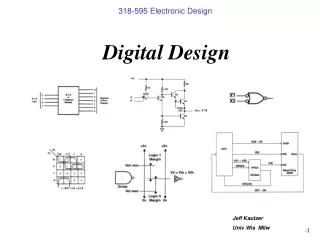
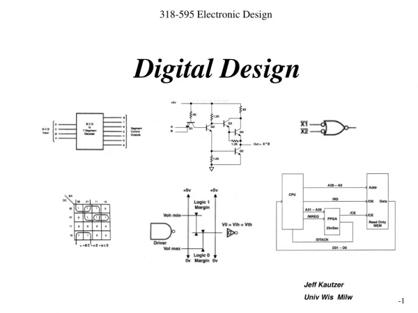
Digital Design. Jeff Kautzer Univ Wis Milw. Review of Medium Scale Integration (MSI) Logic Circuits. Common digital system tasks are commercially available as MSI logic devices in many different TTL and CMOS families

E N D
Digital Design Jeff Kautzer Univ Wis Milw
Review of Medium Scale Integration (MSI) Logic Circuits • Common digital system tasks are commercially available as MSI logic devices in many different TTL and CMOS families • Functions such as decoding/encoding, multiplexing, demultiplexing, comparison, arithmetic, code converting, and data busing
Decoders A decoder accepts a set of inputs that represents a binary number and activates only the output that corresponds to that input number. General decoder diagram
Typically decoders have ENABLE inputs used to control operation • All ENABLE inputs must be satisfied for an output to be active
Enables can be used to cascade into larger decoders Example: Four 74ALS138s forming a 1-of-32 decoder
The 7442 style BCD-to-decimal decoder • One output is active based on the Binary Coded Decimal input value
Counter/decoder combination can be used to provide timing and sequencing operations
Encoders A encoder is a decoder in reverse, that is, it accepts a single active input from an input set, and delivers an N-Bit code corresponding to which input was active. General encoder diagram.
Logic circuit for an octal-to-binary (8-to-3) active lowencoder. For proper operation, only one input should be active at one time.
A priority encoder has special logic to ensure that when two or more inputs are activated, the output code will correspond to the highest-numbered input. 74147 style decimal-to-BCD priority encoder.
Priority encoder application as a switch encoder. NOTE: Switches must be debounced (not shown)!
Priority Encoder Application: Keyboard entry of 3-digit number into storage registers with proper debounce and clear function
Multiplexers A multiplexer (MUX) is a circuit that selects 1 input from a set based on the selection code input. Functional diagram of a digital multiplexer (MUX)
Data Routing MUX Application System for displaying two multidigit BCD counters one at a time.
Parallel-to-Serial MUX Application Parallel-to-serial converter; waveforms for X7X6X5X4X3X2X1X0 = 10110101 JK’s used as Toggle Flip-flop Ripple Counter
Operation Sequencing MUX/Decoder Application Seven-step control sequence Starts by filling tank1, when full it toggles to fill tank 2, etc.
Logic Function Generation MUX Application MUX used to implement a canonical SOP logic function