Download
1 / 19
390 likes | 1.65k Views
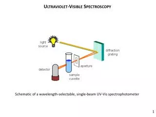
Detectors (UV-Vis) 1. Phototube 2. Photomultiplier Tube (PMT) 3. Si Photodiode 4. Photodiode Array (PDA) 5. Charge Coupled Device (CCD) 6. Charge Injection Device (CID). 200 – 1000 nm 1-10 ns response time 0.01 A/W. 1. Phototube. 110 – 1000 nm 1-10 ns response time 10,000 A/W.

E N D
Detectors (UV-Vis) 1. Phototube 2. Photomultiplier Tube (PMT) 3. Si Photodiode 4. Photodiode Array (PDA) 5. Charge Coupled Device (CCD) 6. Charge Injection Device (CID)
200 – 1000 nm 1-10 ns response time 0.01 A/W 1. Phototube
110 – 1000 nm 1-10 ns response time 10,000 A/W 2. Photomultiplier Tube (PMT)
Si: 3s23p2 Covalent Bonds in Solid Therefore 1/2–filled sp3 ΔE ≤ 2.5 eV (semiconductor) 3. Si Photodiode 4 electrons fill a valence band at 0K At higher T an electron can move to conduction band Leaving a positive hole behind (both are mobile)
Doping Si with a group 5 element (As or Sb) results in extra electrons (n-type). Doping with a group 3 element (In, Ga) results in extra holes (p-type) 3. Si Photodiode
3. Si Photodiode Forward bias (not very useful for spectroscopy)
Reversed Bias: Depletion zone at the junction. Photons may eject electrons and form holes Current proportional to number of photons 3. Si Photodiode
200 – 1000 nm 1-10 ns response time 0.05 A/W 3. Si Photodiode
4. Linear Photodiode Array 200 – 1000 nm 1-10 ns response time 0.05 A/W
200 – 950 nm 1-10 ns response time 0.05 - 1000 A/W 5. Charge Coupled Device (CCD)
Detector Responsivity R(λ) = Current Output (A) Incident Power (W) Gain of the Signal Modifier G = Output Potential (V) Input Current (A)