Download
1 / 26
260 likes | 345 Views
Final presentation on designing and implementing a high-speed communication switch utilizing advanced protocols for optimal transmission rates. Utilizes Stratix II SI Development Kit.

E N D
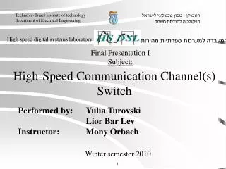
Technion - Israel institute of technology department of Electrical Engineering הטכניון - מכון טכנולוגי לישראלהפקולטה להנדסת חשמל High speed digital systems laboratory המעבדה למערכות ספרתיות מהירות Final Presentation I Subject: High-Speed Communication Channel(s) Switch Performed by: Yulia Turovski Lior Bar Lev Instructor: Mony Orbach Winter semester 2010 1
High speed digital systems laboratory המעבדה למערכות ספרתיות מהירות Outline • Reminder – Motivation and Goal • Stratix II SI Development Kit • Project Basics • SerialLite II • Network & Data Link Packet Format • Architecture and Components • Simulations • Validation Method • Gantt diagram 2
High speed digital systems laboratory המעבדה למערכות ספרתיות מהירות Motivation and Goal • Motivation: • High-speed communication between devices. • Utilizing high frequency achievable with new hardware. • Demand for reliable communication • Goal: • Design & implementation of high speed communication switch. • Use of advanced communication protocols. • Connect between as many devices as possible. • Best transmission rate possible. 2
High speed digital systems laboratory המעבדה למערכות ספרתיות מהירות Stratix II SI Development Kit • The hardware for the project: Stratix II GX Transceiver Signal Integrity Development Board • Clocking: Numerous oscillators, we chose PCI-Express standard 156.25 MHz. • Communication channels: • 4 identical stripline channels - USED • 2 unique channels (microstrip and long trace simulator) – not used • Stratix II GX EP2SGX90EF1152C3 FPGA – 90,960 LE’s, Max Transceiver data rate 6.375Gbps, 4,520K RAM, 192 18X18 Multipliers, 48 DSP blocks, 8 PLLs, 558 I/O pins 2
High speed digital systems laboratory המעבדה למערכות ספרתיות מהירות Stratix II SI Development Kit 2
High speed digital systems laboratory המעבדה למערכות ספרתיות מהירות Project Basics • Communication using board’s transceivers. • Basic element: ALT2GXB MegaCore: • Receiver-transmitter from transfer size (32bit max for 1 lane) to serial interface. • Multiplies core clock to reach desired data rate • Tested thoroughly in previous project • Successfully burnt and tested • Alternative: SerialLite II MegaCore: • Uses ALT2GXB as a component • Adds optional data link services i.e. reliability, CRC, flow control etc. 2
High speed digital systems laboratory המעבדה למערכות ספרתיות מהירות Altera SerialLite II • By documentation, core can act as physical and data link layers of this project. • Use was forsaken due to technical difficulties. • Instead: • using the physical layer from a previous project • created our own data link layer. • Simple but sufficient GBN protocol of fixed window (10^(-12) error probability). 2
High speed digital systems laboratory המעבדה למערכות ספרתיות מהירות Network Layer Format • Network Layer (routing): • Constant packet size of 128 bytes • Variable packet size: • Would be more efficient and versatile • Complicates the design significantly • Constant packet size: • Simplifies design • Enables determining quality of service, i.e. number of packets in memory • Reminder: Mid-semester presentation showed 32-byte packets, which were increased to minimize overhead. • but not so much, as needs to fit in FPGA! Packet Address 8bit Data 123Byte 32bit CRC 2
High speed digital systems laboratory המעבדה למערכות ספרתיות מהירות Data Link Format & Protocol • Data Link Layer (reliability over single connection): • Simple GBN with constant generic window <=7 • GBN: • Provides enough reliability • Simplifies the design (but is still not trivial) • Ack for every message – 1/33 additional overhead • Alternative – Selective Repeat • Provides same reliability • Requires Nack and discards a packet, but only for bad messages – very low probability (10^-9) • Project demand was GBN. Frame FF+msgnum (4 byte) Network layer packet (128 byte) F0+msgnum (4 byte) ACK 2
High speed digital systems laboratory המעבדה למערכות ספרתיות מהירות Architecture Diagram ROUTER 128 128 128 ALTGX ALTGX ALTGX TRNS TRNS TRNS OUTBUF OUTBUF OUTBUF 32 32 32 128 ALTGX TRNS OUTBUF 32 INBUF INBUF INBUF INBUF 32 RECV 128 SPLIT INBUF 32 32 32 RECV RECV RECV SPLIT SPLIT SPLIT 128 128 128 INBUF Trans Mem INBUF INBUF INBUF INBUF INBUF INBUF INBUF Trans Mem Trans Mem Trans Mem INBUF INBUF INBUF 3
High speed digital systems laboratory המעבדה למערכות ספרתיות מהירות Architecture Diagram ROUTER 128 ALTGX TRNS OUTBUF 32 INBUF 32 RECV 128 SPLIT INBUF INBUF Trans Mem INBUF 3
High speed digital systems laboratory המעבדה למערכות ספרתיות מהירות Architecture Notes • Serial interfaces send 32 bits on every channel every clock • The switch core (between receiver and transmitter) sends 128 bits every clock • Reason: To compensate for changing routes • Serial interfaces always send to same line • In-switch routing may be occupied due to routing options • i.e. all ports transmit to the same port • X4 rate for 4 ports means no congestion in switching (avg) • Disadvantages: • Complicates design • Lots of logic for parallel data transfer (128-bit muxes) 2
High speed digital systems laboratory המעבדה למערכות ספרתיות מהירות Architecture Notes • Many ways to implement queues, fairness, buffering\GBN. • Simple FIFO per input: • Seems memory efficient – single queue • Packets to full destinations block packets to others not full • - which fills buffers => more memory! • Single non-FIFO per input: • Most memory efficient – single buffer with bypasses • Requires memory management – very complicated • FIFO per input per destination: • Most memory-consuming – even when some directions idle • Most parallel – actually a switch to each destination • Each FIFO can be smaller to minimize consumption • But needed to deal with pre-switch congestion 2
High speed digital systems laboratory המעבדה למערכות ספרתיות מהירות ALTGX Block • The physical layer of the switch. • Parallel interface is 32-bit wide, chosen clock is the PCI-Express standard 156.25 (multiplied) • Serial interface is a multiple of said clock, up to 6.25GB • Used in previous projects • Successfully synthesized and burnt onto our FPGA • ALTGX is a sub-block of the forsaken SerialLite megacore ALTGX
High speed digital systems laboratory המעבדה למערכות ספרתיות מהירות Receiver Block • The receiver side of the Data Link layer • Receives 32 bits of data every clock • Packs data to 128-bit words • CRC check • Informs transmitter of: • Good packets to ACK • Received ACKS to forward GBN window • Outputs the virtual 8-bit address to translation memory • Result 2-bit port is forwarded to next block with some delay RECV
High speed digital systems laboratory המעבדה למערכות ספרתיות מהירות SPLIT Block • Destination port arrives 3-clocks late from translation memory • Unit includes a shift-register to synchronize • Outputs the data to all 4 In Buffers • WREN is enabled for the destination port only SPLIT
High speed digital systems laboratory המעבדה למערכות ספרתיות מהירות INBUF Block • 16 such buffers – one per input-output pair • When receives signal from router, sends 8 128-bit words in 8 clocks • Uses dual-port ram • FIFO INBUF
High speed digital systems laboratory המעבדה למערכות ספרתיות מהירות OUTBUF Block • 4 such buffers – one per output • Mux in entrance to buffer • When receives signal from router, stores 8 128-bit words in 8 clocks • Mux transfers the data from the INBUF activated by router • Uses dual-port ram • FIFO • Data is read by transmitter • When finished, entries are invalidated OUTBUF
High speed digital systems laboratory המעבדה למערכות ספרתיות מהירות ROUTER Block • Chooses an input entry for each available output buffer and starts transmission at both ends • Fairness using Round Robin for start index ROUTER • Algorithm: • Hold start index (Round Robin) • For each output port j • For each in port i (start index to N and then 1 to start-1) • Each buffer offers first message for each output port (4) • If size(i)>Max • Max=size(i), Pchoose(j)=i • Transfer Pchoose[j] 4
High speed digital systems laboratory המעבדה למערכות ספרתיות מהירות Transmitter Block • The transmitter side of the Data Link layer • Reads 128-bit words directly from OUTBUF • Adds 32 bit header • Transmits 32 bits of data every clock • Handles GBN protocol window for the port • Actions: • Advance window when receives ACK • Sends ACK as asked by receiver TRNS
High speed digital systems laboratory המעבדה למערכות ספרתיות מהירות Architecture Diagram ROUTER 128 ALTGX TRNS OUTBUF 32 INBUF 32 RECV 128 SPLIT INBUF INBUF Trans Mem INBUF 3
High speed digital systems laboratory המעבדה למערכות ספרתיות מהירות Architecture Diagram ROUTER 128 128 128 ALTGX ALTGX ALTGX TRNS TRNS TRNS OUTBUF OUTBUF OUTBUF 32 32 32 128 ALTGX TRNS OUTBUF 32 INBUF INBUF INBUF INBUF 32 RECV 128 SPLIT INBUF 32 32 32 RECV RECV RECV SPLIT SPLIT SPLIT 128 128 128 INBUF Trans Mem INBUF INBUF INBUF INBUF INBUF INBUF INBUF Trans Mem Trans Mem Trans Mem INBUF INBUF INBUF 3
High speed digital systems laboratory המעבדה למערכות ספרתיות מהירות Simulations • … 8
High speed digital systems laboratory המעבדה למערכות ספרתיות מהירות Validation Method • 4 transmitters with pre-initialized dual port rams • Simple data validation control (to keep track of number of packets sent) • Various scenarios can be implemented this way • Measure latency • Measure Throughput • Parallel transmission • Congestion – all ports transmit to same port • Deliberate errors • Output the data through JTAG (as told by our instructor) 8
High speed digital systems laboratory המעבדה למערכות ספרתיות מהירות Validation Method (2) Test device Switch Valid control Port I Port I TRNS OUT RECV Port II Port II TRNS RECV OUT Port III Port III TRNS OUT RECV Port IV Port IV TRNS RECV OUT 2
High speed digital systems laboratory המעבדה למערכות ספרתיות מהירות Project Schedule Minimum goal: showing one or two tests on board Maximum goal: showing all tests planned 9