8 Bit ALU
EE 166 Design Project San Jose State University. 8 Bit ALU. Roger Flores Brian Silva Chris Tran Harizo Yawary Advisor: Dr. Parent May 2006. Agenda. Abstract: Specifications Introduction Why: 8 Bit Arithmetic Logic Unit (ALU) Simple Theory: Block diagram

8 Bit ALU
E N D
Presentation Transcript
EE 166 Design ProjectSan Jose State University 8 Bit ALU • Roger Flores • Brian Silva • Chris Tran • Harizo Yawary Advisor: Dr. Parent May 2006
Agenda • Abstract: Specifications • Introduction • Why: 8 Bit Arithmetic Logic Unit (ALU) • Simple Theory: Block diagram • Back Ground information: Han-Carlson • Summary of Results • Project Details • Results • Time Analysis • Conclusions
Abstract • Design an 8 bit ALU with 4 functions: 1. AND 2. OR 3. XOR 4. Han Carlson Adder • Maximum propagation delay: 5 ns • Area: 981.9µm ×1185.6µm = 1.16µm2 • Frequency: 200 MHz
Introduction • ALU chip design involves changing the logic function into equivalent circuits and creating fast switching networks. • ALU chip performs addition and basic logical operations such as AND, OR, and XOR. • Han-Carlson adder structure has minimum logic depth, resulting in a fast adder but with a large area. • Control Pins AOI for Propagate: P = C0A’B’ + C1A’B + C2AB’ + C3AB AOI for Generate: G = C4AB + C5AB’ +C6A’B + C7A’B’
Design Block Diagram Sketch Schematics Finish Find Euler Path Measure delay time Draw stick Diagram Verify functionality Calculate Wn Wp for each block Run verilog simulation Run Spice simulation to fix Wn, Wp Run analog simulation Draw schematic for each block Run DRC, LVS, simulation for 8-bit ALU Layout for each small blocks Run DRC, LVS, simulation for small blocks Combine all Blocks to make 8-bit ALU
8 Bit ALU - Schematics Input D FF Han-Carlson Output D FF
Final 8 Bit ALU – LVS Report Yes! Layout = Schematic
Verification Add Logic OR Logic
XOR Logic Adder Logic
Project Summary • Total of 27 input and 9 output pins • Total of 34 D Flip Flops • Designed schematics and layouts for And gate, OR gate, XOR gate and Han-Carlson, Adder, MUX based FF, PG and GG using Cadence tools. • Tested each schematic with test bench • DRC and LVS passed for each component • Successfully designed a four function eight bit ALU. • Our calculated time delay was 5.14 ns compared to the spec of 5ns. (2.7% error)
Lessons Learned • Start early • Educate everyone in the group • Work together Time Analysis • Research Design 8 Days • Design and Verify Total 4 Weeks • Logic 5 Days • Each Gate Schematics 4 Days • Each Gate Layout 4 Days • Final Schematics 3 Days • Final Layout 3 Days • Test Bench 1 Day • Verify NC Verilog 1 Day
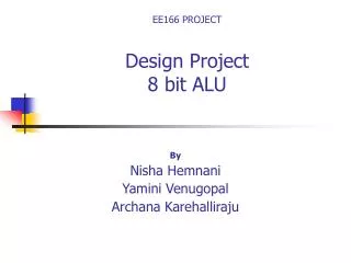
Acknowledgements • Thanks to Dr. Parent for steering us to the right direction with his recommendations. • Thanks to our friends that took this class last semester. • Thanks to Cadence Design Systems for the VLSI lab • Thanks to Synopsys for Software donation