Download
1 / 38
380 likes | 575 Views
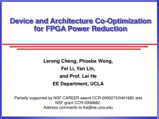
Device and Architecture Co-Optimization for FPGA Power Reduction. Lerong Cheng, Phoebe Wong, Fei Li, Yan Lin, and Prof. Lei He EE Department, UCLA Partially supported by NSF CAREER award CCR-0093273/0401682 and NSF grant CCR-0306682. Address comments to lhe@ee.ucla.edu. Outline.

E N D
Device and Architecture Co-Optimization for FPGA Power Reduction Lerong Cheng, Phoebe Wong, Fei Li, Yan Lin, and Prof. Lei He EE Department, UCLA Partially supported by NSF CAREER award CCR-0093273/0401682 and NSF grant CCR-0306682. Address comments to lhe@ee.ucla.edu
Outline • Background and motivation • Trace-based power and delay estimation • Device and architecture co-optimization • Conclusion
Connection box Switch box 9 (12, 7) 8 7 (10, 7) (12, 6) (10, 3) Total FPGA Energy (nJ/cycle) (12, 3) 6 (8, 7) (10, 6) (8, 3) (8, 6) (12, 5) (6, 7) 5 (6, 3) (6, 6) (6, 5) (10, 5) (8, 5) (6, 4) 4 (12, 4) (10, 4) (8, 4) 3 9 10 11 12 13 14 15 16 17 I/O pad Logic block Critical Path Delay (ns) Evaluation of Conventional FPGA Architecture • LUT size and cluster size have been evaluated for conventional FPGA • performance and area [Ahmed et al, ISFPGA’00] • power and performance [Li et al, ISFPGA ‘03] • Architecture tuning leads to 2.8X energy difference and1.5X delay difference Island style FPGA architecture Evaluation result
Vdd programmable logic block Conventional FPGA Vdd programmable FPGA High Vdd Logic block Low Vdd logic block Evaluation of Low-Power FPGA Architecture • Field programmable dual-vdd for power reduction [Lin et al, ISFPGA’05] • Applying field programmable dual Vdd reduces energy-delay product by 49%
Parasitic Extraction Arch Spec Power Evaluation Methodology Benchmark circuits Logic Optimization(SIS) Tech-Mapping (RASP) Timing-Driven Packing (TV-Pack) Cycle-accurate Power Simulator (Psim) Placement & Routing (VPR) Area Delay
Impact of Device Tuning • All the previous work only considers architecture tuning • Device tuning leads to 84X power difference and 12X delay difference • It is necessary to perform device tuning and architecture tuning simultaneously
Challenge of Device and Architecture Co-Optimization • We consider the following architecture and device parameters during our co-optimization: • Architecture parameters: • Cluster size (N) • LUT size (K) • Device parameters: • Supply voltage (Vdd) • Threshold voltage (Vt) • Hyper-architecture (hyper-arch) is the combination of the device and architecture parameters. • Large number of hyper-arch combinations • VPR and Psim are too slow to deal with such large numberof experiments • Need fast yet accurate power and delay estimation
Outline • Back ground and motivation • Trace-based power and delay estimation • Trace collection • Trace based power and delay model • Accuracy and efficiency verification of Trace-based estimator • Device and architecture co-optimization • Conclusion
Trace Collection Circuit element statistics • Assume trace information will remain the same when device setting changes Critical path structure VPR and Psim Short circuit power ratio Trace Ptrace Switching activity Area
Trace Base Estimation (Ptrace) Framework Device independent Ptrace Trace Chip level delay, power, and area Device dependent Circuit level delay and power
Outline • Back ground and motivation • Trace-based power and delay estimation • Trace collection • Trace based power and delay model • Accuracy and efficiency verification of Trace-based estimator • Device and architecture co-optimization • Conclusion
Delay Model in VPR • Delay is calculated for each path as • Nip is number of type i elements in the path and Di is delay oftype i element • Delay of the logic elements is measured by SPICE simulation • Elmore delay is used for interconnect wire segments • Critical path is the path with longest delay
Delay in Ptrace • Obtain the path structure of a set of longest circuit paths • Assume that when device setting changes, the new critical path is still among the set of longest paths. • Delay computation: Trace information Device dependent parameters
Dynamic Power Model • Psim • Switch power • Switching activity is measured by timing simulation for each node • Si is the average switching activity • Short circuit power • αsc is calculated for each node • Ptrace • Switch power • Short circuit power • αsc is the average short circuit power ratio for the whole circuit Trace information Device dependent parameters
Static Power Model • Psim • Without power gating • With power gating • Ptrace • Without power gating • With power gating Trace information Device dependent parameters
Outline • Back ground and motivation • Trace-based power and delay estimation • Trace collection • Trace based power and delay model • Accuracy and efficiency verification of Trace-based estimator • Device and architecture co-optimization • Conclusion
Experiment Setting • Collect trace using ITRS 70nm technology, but apply to both 100nm and 70nm technologies • 20 MCNC benchmarks • Assume each benchmark works in its highest possible frequency • Power and delay are computed as geometric mean of20 benchmarks. • Evaluation range
Accuracy • Average power error is 3.4%. • Average delay error is 6.4%. • Delay error is due to Ptrace ignores the impact of path branches that considered in VPR
Runtime • VPR and Psim for one device setting • five days on eight 1.2GHz Intel Xeon servers • Ptrace for 20 device settings • 80 seconds on one 1.2GHz Intel Xeon server
Outline • Back ground and motivation • Trace-based power and delay estimation • Device and architecture co-optimization • Energy and delay tradeoff • ED and area tradeoff • Comparison between classes • Comparison between device tuning and architecture tuning • Conclusion
Architectures Classes to be Evaluated • Hyper-architecture classes • Baseline case • Vdd suggested by ITRS • Architecture same as Xilinx Virtex-II™. • Vt optimized by our method with respect to the above architecture and Vdd
Outline • Back ground and motivation • Trace-based power and delay estimation • Device and architecture co-optimization • Energy and delay tradeoff • ED and area tradeoff • Comparison between classes • Comparison between device tuning and architecture tuning • Conclusion
Energy and Delay Tradeoff • Dominant hyper-arch • Hyper-arch B is inferior to A if A has less energy and smaller delay than B. • Dominant hyper-archs (dom-arch) are the hyper-archs that are NOT inferior to any other hyper-archs.
Energy and Delay Tradeoff • Hetero-Vt can reduce power • Power gating reduces more leakage power than hetero-Vt • Hetero-Vt has less impact when power gating is applied
Min-ED Hyper-Arch • To achieve the best energy and delay tradeoff, we find out the hyper-arch with the minimum energy and delay product (ED) • Compared to the baseline, the min-ED hyper-arch of the conventional FPGA (Homo-Vt) reduces ED by 13.4% • For the Hetero-Vt class, ED is reduced by 20.5% • If power gating is applied, ED can be reduced by up to 59.0%
Outline • Back ground and motivation • Trace-based power and delay estimation • Device and architecture co-optimization • Energy and delay tradeoff • ED and area tradeoff • Comparison between classes • Comparison between device tuning and architecture tuning • Conclusion
ED and area Tradeoff • Architecture tuning has great impact on area. • To achieve the best area and ED tradeoff, we find the hyper-arch with the minimum product of area, energy and delay (AED)
ED Area Tradeoff for Classes without Power Gating • Compared to the min-ED hyper arch, the min-AED hyper-arch significantly reduce area with a small ED increase
Sleep Transistor Size Tuning • When Power gating is applied, sleep transistors may increase area • The larger the sleep transistor size, the smaller the delay • Sleep transistor size tuning: • Area overhead introduced by sleep transistors of logic blocks is negligible. • We consider 2X, 4X, 7X and 10X PMOS as sleep transistor for switch buffer
ED Area Tradeoff for Classes with Power Gating • The area reduction achieved by device and architecture co-optimization compensates the area overhead introduced by sleep transistors
Min-AED Hyper-Arch • Compared to the baseline, the min-AED hyper-arch in the conventional FPGA class can reduce area by 20% and ED by 12.3% • In the Hetero-Vt class, ED is reduced by 20.8% and area is reduced by 23% compared to the baseline • If power gating is applied, ED is reduced by 54.6% and area is reduced by 8.3%
Outline • Back ground and motivation • Trace-based power and delay estimation • Device and architecture co-optimization • Energy and delay tradeoff • ED and area tradeoff • Comparison between classes • Comparison between device tuning and architecture tuning • Conclusion
Comparison Between Classes in Similar Performance Range • Vt for logic block is lower than Vt for interconnect • Vt for classes with power gating is lower
Outline • Back ground and motivation • Trace-based power and delay estimation • Device and architecture co-optimization • Energy and delay tradeoff • ED and area tradeoff • Comparison between classes • Comparison between device tuning and architecture tuning • Conclusion
Dom-Archs under Different Device Settings • For a given device setting architecture tuning changes delay and energy in a smaller range • Device tuning has a much more impact on delay and energy
Outline • Back ground and motivation • Trace-based power and delay estimation • Device and architecture co-optimization • Conclusion
Conclusion and Discussion • Trace-based estimator provides efficient and accurate FPGA power and delay estimation • Average power error is 3.4% and average delay error is 6.1% • Device and architecture co-optimization reduces ED by 20.5% and area by 23.3% when there is no power gating • With power gating, device and architecture co-optimization reduces ED by 54.6% and area by 8.3% • Device tuning has a more significant impact on delay and power than architecture tuning does • In recent research, Ptrace has been extended to consider leakage and timing yield with process variations