Basic FPGA Architecture
This module offers an in-depth exploration of FPGA architecture, focusing on the essential resources available in Xilinx devices like the Virtex-II, Spartan-3, and Virtex-4 families. Participants will learn to identify key architectural features, including slice resources, I/O resources, and memory, and understand the differences between various device families. We will also cover advanced features such as carry logic, multiplexing, and flexible sequential elements, laying a solid foundation for FPGA design and application development.

Basic FPGA Architecture
E N D
Presentation Transcript
Objectives After completing this module, you will be able to: • Identify the basic architectural resources of the Virtex™-II FPGA • List the differences between the Virtex-II, Virtex-II Pro, Spartan™-3, and Spartan-3E devices • List the new and enhanced features of the new Virtex-4 device family
Outline • Overview • Slice Resources • I/O Resources • Memory and Clocking • Spartan-3, Spartan-3E, and Virtex-II Pro Features • Virtex-4 Features • Summary • Appendix
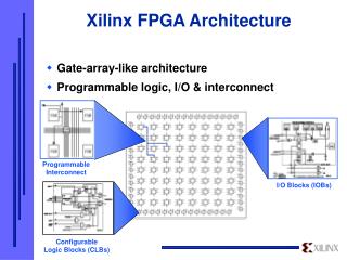
Overview • All Xilinx FPGAs contain the same basic resources • Slices (grouped into CLBs) • Contain combinatorial logic and register resources • IOBs • Interface between the FPGA and the outside world • Programmable interconnect • Other resources • Memory • Multipliers • Global clock buffers • Boundary scan logic
Outline • Overview • Slice Resources • I/O Resources • Memory and Clocking • Spartan-3, Spartan-3E, and Virtex-II Pro Features • Virtex-4 Features • Summary • Appendix
BUFT BUF T Slices and CLBs • Each Virtex-II CLB contains four slices • Local routing provides feedback between slices in the same CLB, and it provides routing to neighboring CLBs • A switch matrix provides access to general routing resources COUT COUT Switch Matrix Slice S3 Slice S2 SHIFT Slice S1 Slice S0 Local Routing CIN CIN
Simplified Slice Structure • Each slice has four outputs • Two registered outputs, two non-registered outputs • Two BUFTs associated with each CLB, accessible by all 16 CLB outputs • Carry logic runs vertically, up only • Two independent carry chains per CLB Slice 0 LUT PRE Carry D Q CE CLR LUT Carry PRE D Q CE CLR
Detailed Slice Structure • The next few slides discuss the slice features • LUTs • MUXF5, MUXF6, MUXF7, MUXF8 (only the F5 and F6 MUX are shown in this diagram) • Carry Logic • MULT_ANDs • Sequential Elements
Combinatorial Logic A B Z C D Look-Up Tables • Combinatorial logic is stored in Look-Up Tables (LUTs) • Also called Function Generators (FGs) • Capacity is limited by the number of inputs, not by the complexity • Delay through the LUT is constant
F8 F5 F6 F5 F7 F5 F6 F5 Connecting Look-Up Tables MUXF8 combines the two MUXF7 outputs (from the CLB above or below) CLB Slice S3 MUXF6 combines slices S2 and S3 Slice S2 MUXF7 combines the two MUXF6 outputs Slice S1 MUXF6 combines slices S0 and S1 Slice S0 MUXF5 combines LUTs in each slice
COUT COUT To S0 of the next CLB To CIN of S2 of the next CLB SLICE S3 First Carry Chain CIN COUT SLICE S2 SLICE S1 CIN Second Carry Chain COUT SLICE S0 CIN CIN CLB Fast Carry Logic • Simple, fast, and complete arithmetic Logic • Dedicated XOR gate for single-level sum completion • Uses dedicated routing resources • All synthesis tools can infer carry logic
MULT_AND Gate • Highly efficient multiply and add implementation • Earlier FPGA architectures require two LUTs per bit to perform the multiplication and addition • The MULT_AND gate enables an area reduction by performing the multiply and the add in one LUT per bit LUT A CY_MUX CO S DI CI CY_XOR MULT_AND A x B LUT B LUT
_1 FDRSE D S Q CE R FDCPE D PRE Q CE CLR LDCPE D PRE Q CE G CLR Flexible Sequential Elements • Either flip-flops or latches • Two in each slice; eight in each CLB • Inputs come from LUTs or from an independent CLB input • Separate set and reset controls • Can be synchronous or asynchronous • All controls are shared within a slice • Control signals can be inverted locally within a slice
D Q CE D Q CE D Q CE D Q LUT CE Shift Register LUT (SRL16CE) • Dynamically addressable serial shift registers • Maximum delay of 16 clock cycles per LUT (128 per CLB) • Cascadable to other LUTs or CLBs for longer shift registers • Dedicated connection from Q15 to D input of the next SRL16CE • Shift register length can be changed asynchronously by toggling address A LUT D CE CLK Q A[3:0] Q15 (cascade out)
64 64 Shift Register LUT Example • The SRL can be used to create a No Operation (NOP) • This example uses 64 LUTs (8 CLBs) to replace 576 flip-flops (72 CLBs) and associated routing and delays 12 Cycles Operation A Operation B 4 Cycles 8 Cycles Operation C Operation D - NOP 3 Cycles 9 Cycles Paths are Statically Balanced 12 Cycles
Outline • Overview • Slice Resources • I/O Resources • Memory and Clocking • Spartan-3, Spartan-3E, and Virtex-II Pro Features • Virtex-4 Features • Summary • Appendix
IOB Element • Input path • Two DDR registers • Output path • Two DDR registers • Two 3-state enable DDR registers • Separate clocks and clock enables for I and O • Set and reset signals are shared IOB Input Reg DDR MUX Reg OCK1 ICK1 Reg Reg 3-state OCK2 ICK2 Reg DDR MUX PAD OCK1 Reg Output OCK2
SelectIO Standard • Allows direct connections to external signals of varied voltages and thresholds • Optimizes the speed/noise tradeoff • Saves having to place interface components onto your board • Differential signaling standards • LVDS, BLVDS, ULVDS • LDT • LVPECL • Single-ended I/O standards • LVTTL, LVCMOS (3.3V, 2.5V, 1.8V, and 1.5V) • PCI-X at 133 MHz, PCI (3.3V at 33 MHz and 66 MHz) • GTL, GTLP • and more!
Digital ControlledImpedance (DCI) • DCI provides • Output drivers that match the impedance of the traces • On-chip termination for receivers and transmitters • DCI advantages • Improves signal integrity by eliminating stub reflections • Reduces board routing complexity and component count by eliminating external resistors • Eliminates the effects of temperature, voltage, and process variations by using an internal feedback circuit
Outline • Overview • Slice Resources • I/O Resources • Memory and Clocking • Spartan-3, Spartan-3E, and Virtex-II Pro Features • Virtex-4 Features • Summary • Appendix
Other Virtex-II Features • Distributed RAM and block RAM • Distributed RAM uses the CLB resources (1 LUT = 16 RAM bits) • Block RAM is a dedicated resources on the device (18-kb blocks) • Dedicated 18 x 18 multipliers next to block RAMs • Clock management resources • Sixteen dedicated global clock multiplexers • Digital Clock Managers (DCMs)
Distributed SelectRAM Resources • Uses a LUT in a slice as memory • Synchronous write • Asynchronous read • Accompanying flip-flops can be used to create synchronous read • RAM and ROM are initialized duringconfiguration • Data can be written to RAMafter configuration • Emulated dual-port RAM • One read/write port • One read-only port RAM16X1S D LUT WE WCLK A0 O A1 A2 A3 RAM32X1S RAM16X1D D D WE WE Slice WCLK WCLK A0 O A0 SPO LUT A1 A1 A2 A2 A3 A3 A4 DPRA0 DPO DPRA1 DPRA2 LUT DPRA3
Block SelectRAM Resources • Up to 3.5 Mb of RAM in 18-kb blocks • Synchronous read and write • True dual-port memory • Each port has synchronous read and write capability • Different clocks for each port • Supports initial values • Synchronous reset on output latches • Supports parity bits • One parity bit per eight data bits 18-kb block SelectRAM memory DIA DIPA ADDRA WEA ENA SSRA DOA CLKA DOPA DIB DIPB ADDRB WEB ENB SSRB DOB CLKB DOPB
Dedicated Multiplier Blocks • 18-bit twos complement signed operation • Optimized to implement Multiply and Accumulate functions • Multipliers are physically located next to block SelectRAM™ memory 18 x 18 Multiplier Data_A (18 bits) Output (36 bits) Data_B (18 bits)
Global Clock Routing Resources • Sixteen dedicated global clock multiplexers • Eight on the top-center of the die, eight on the bottom-center • Driven by a clock input pad, a DCM, or local routing • Global clock multiplexers provide the following: • Traditional clock buffer (BUFG) function • Global clock enable capability (BUFGCE) • Glitch-free switching between clock signals (BUFGMUX) • Up to eight clock nets can be used in each clock region of the device • Each device contains four or more clock regions
Digital Clock Manager (DCM) • Up to twelve DCMs per device • Located on the top and bottom edges of the die • Driven by clock input pads • DCMs provide the following: • Delay-Locked Loop (DLL) • Digital Frequency Synthesizer (DFS) • Digital Phase Shifter (DPS) • Up to four outputs of each DCM can drive onto global clock buffers • All DCM outputs can drive general routing
Outline • Overview • Slice Resources • I/O Resources • Memory and Clocking • Spartan-3, Spartan-3E, and Virtex-II Pro Features • Virtex-4 Features • Summary • Appendix
Lower cost Smaller process = lower core voltage .09 micron versus .15 micron Vccint = 1.2V versus 1.5V Different I/O standard support New standards: 1.2V LVCMOS, 1.8V HSTL, and SSTL Default is LVCMOS, versus LVTTL More I/O pins per package Only one-half of the slices support RAM or SRL16s (SLICEM) Fewer block RAMs and multiplier blocks Same size and functionality Eight global clock multiplexers Two or four DCM blocks No internal 3-state buffers 3-state buffers are in the I/O Spartan-3 versus Virtex-II
SLICEM and SLICEL • Each Spartan™-3 CLB contains four slices • Similar to the Virtex™-II • Slices are grouped in pairs • Left-hand SLICEM (Memory) • LUTs can be configured as memory or SRL16 • Right-hand SLICEL (Logic) • LUT can be used as logic only Right-Hand SLICEL Left-Hand SLICEM COUT COUT Switch Matrix Slice X1Y1 Slice X1Y0 SHIFTIN Slice X0Y1 Slice X0Y0 Fast Connects CIN CIN SHIFTOUT
More gates per I/O than Spartan-3 Removed some I/O standards Higher-drive LVCMOS GTL, GTLP SSTL2_II HSTL_II_18, HSTL_I, HSTL_III LVDS_EXT, ULVDS DDR Cascade Internal data is presented on a single clock edge 16 BUFGMUXes on left and right sides Drive half the chip only In addition to eight global clocks Pipelined multipliers Additional configuration modes SPI, BPI Multi-Boot mode Spartan-3E Features
Virtex-II Pro Features • 0.13 micron process • Up to 24 RocketIO™ Multi-Gigabit Transceiver (MGT) blocks • Serializer and deserializer (SERDES) • Fibre Channel, Gigabit Ethernet, XAUI, Infiniband compliant transceivers, and others • 8-, 16-, and 32-bit selectable FPGA interface • 8B/10B encoder and decoder • PowerPC™ RISC processor blocks • Thirty-two 32-bit General Purpose Registers (GPRs) • Low power consumption: 0.9mW/MHz • IBM CoreConnect bus architecture support
Outline • Overview • Slice Resources • I/O Resources • Memory and Clocking • Spartan-3, Spartan-3E, and Virtex-II Pro Features • Virtex-4 Features • Summary • Appendix
Virtex-4 Features • New features • Dedicated DSP blocks • Phase-matched clock dividers (PMCD) • SERDES built into the Virtex™-4 SelectIO™ standard • Dynamic reconfiguration port (DRP) • Enhanced features • Block RAM can be configured as a FIFO • Advanced clocking networks, including regional clock buffers and source- synchronous support • 11.1 Gbps RocketIO™ Multi-Gigabit Transceiver (MGT) blocks • Enhanced PowerPC™ processor blocks
Outline • Overview • Slice Resources • I/O Resources • Memory and Clocking • Spartan-3, Spartan-3E, and Virtex-II Pro Features • Virtex-4 Features • Summary • Appendix
Review Questions • List the primary slice features • List the three ways a LUT can be configured
Answers • List the primary slice features • Look-up tables and function generators (two per slice, eight per CLB) • Registers (two per slice, eight per CLB) • Dedicated multiplexers (MUXF5, MUXF6, MUXF7, MUXF8) • Carry logic • MULT_AND gate • List the three ways a LUT can be configured • Combinatorial logic • Shift register (SRL16CE) • Distributed memory
Summary • Slices contain LUTs, registers, and carry logic • LUTs are connected with dedicated multiplexers and carry logic • LUTs can be configured as shift registers or memory • IOBs contain DDR registers • SelectIO™ standards and DCI enable direct connection to multiple I/O standards while reducing component count • Virtex™-II memory resources include the following: • Distributed SelectRAM™ resources and distributed SelectROM (uses CLB LUTs) • 18-kb block SelectRAM resources
Summary • The Virtex™-II devices contain dedicated 18x18 multipliers next to each block SelectRAM™ resource • Digital clock managers provide the following: • Delay-Locked Loop (DLL) • Digital Frequency Synthesizer (DFS) • Digital Phase Shifter (DPS)
Where Can I Learn More? • User Guides • www.xilinx.com Documentation User Guides • Application Notes • www.xilinx.com Documentation Application Notes • Education resources • Designing with the Virtex-4Family course • Spartan-3E Architecture free Recorded e-Learning