Optimal Integration of New Pixel Layout for TPAC1.1 Progress
This project update includes adjustments to diodes, guard rings, resistor and monostable layouts to enhance performance. The new SRAM layout now includes additional bits. Further optimizations are underway, with a focus on noise analysis and pixel coupling theories.

Optimal Integration of New Pixel Layout for TPAC1.1 Progress
E N D
Presentation Transcript
TPAC1.1 progress Jamie C 4th June 2008
Original pixel layout • Cdiode = 11.4 fF
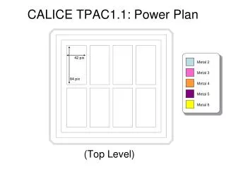
(Current) New Pixel Layout • Adjusted path to diodes • Adjusted guard ring to path • Compacted resistor layout • Compacted monostable layout • Separated monostable power • supply from dco power net • New SRAM layout + 2 bits • 2 extra trim bits (33 transistors) • Cdiode = 12.06 fF • Some connecting routing to do • Some LVS and DRC still to do • Internal analog parts untouched
New pixel NW/DPW layout • Same DPW shape as TPAC1 • New SRAM cells do just fit within • design rules
preShape GAIN TPAC1 Same resistor dimensions TPAC1.1 • Two self-consistent possibilities • Was not picked up in TPAC1 design • Calibre not used for LVS • No explicit cross-check of resistor dimensions • Reported to foundry – awaiting comment • The only hi-res poly resistors in the design are in preShape pixels
Effect of smaller resistance 140μV/e- Reduced Resistances 99μV/e- Original Design e- per diode Ignore: ymax formula picks up reset injection from elsewhere in simulation
Summary Noise analysis setup: Integrated over 10-10Mhz, DIFF_OUT wrt DIFF_IN, 1.8x1.8um diodes, spectre model version 3.1
Lengthening the resistor? • Retain 7 bits SRAM + 6 bits trim • Additional ~0.9MΩ in remaining space 3.6MΩ • Drop to 6 bits of SRAM + 5 bits trim • May be possible (subject to routing) 4MΩ • Original 5 bits of SRAM + 4 bits trim • 4MΩ resistor possible VERY APPROXIMATE ESTIMATES!
Pixel Coupling Theories • (2nd) Comparator & Monostable share power supply VDD1V8dco • Possible coupling from monostable of one pixel to comparator of next (causing comparator to switch) • If this is true… the coupling effect might show a dependence on IOUTBIAS12… 5k variable resistor instead of T1 mod… (nom value 2k2) • VDD1V8mso power net is now unused (preSample pixels only) • this could be re-used in TPAC1.1 to separate those comparator & monostable supplies
Hi-Res Epi (w.r.t. the sensor electronics) • More signal, faster collection etc… • DPW required under all circuits to avoid redesign with larger nwell spacing rules • Circuit operation should be unaffected by DPW • Charge deposited anywhere will collect at edge pixels • Place a NWELL guard ring around the pixels • Collect charge deposited elsewhere • Slight edge effect to array should be limited to outer-most pixels • Separate pins (can re-use VRST net) can be used to monitor current • Quick evaluation suggests there is room for such a guard ring • Not in array centre?