Download
1 / 19
190 likes | 531 Views
Using System-on-a- Chip as a Vehicle for VLSI Design Education . Andrew Laffely and Wayne Burleson Electrical and Computer Engineering University of Massachusetts Amherst {alaffely,burleson}@ecs.umass.edu.

E N D
Using System-on-a-Chip as a Vehicle for VLSI Design Education Andrew Laffely and Wayne Burleson Electrical and Computer Engineering University of Massachusetts Amherst {alaffely,burleson}@ecs.umass.edu This material is based upon work supported by the National Science Foundation under Grant No. 9988238 and SRC Tasks 766 and 1075 Burleson, UMASS
Challenges in VLSI Education • Advancing Processing Technology • Higher level design tools • Realistic yet tractable design projects • Preparation for jobs in semiconductor and other sectors. • Making best use of faculty/student time and university resources Burleson/UMASS
ECE 559/659: VLSI Design Project (10 grads, 20 seniors) • Learn design process for a complex VLSI in deep sub-micron CMOS • Learn VLSI design skills and tools, including working in teams • Learn about a particular application component and its VLSI implementation • Learn to present formal design reviews using oral, written, graphical and web-based techniques Course Objectives: Burleson/UMASS
Key Aspects of the Course • aSoC (home-grown SoC platform) • Provides a unifying framework to class • Allows for subdivision but inter-relation of projects • Interesting cutting edge architecture based on NSF- and SRC-funded research at UMASS and elsewhere • Covers many aspects of VLSI Design • Realistic constraints on area, timing, power and I/O • Graduate and undergraduate teamwork • Graduate students provide leadership, motivation and experience • Commercial tools and design flow • Review-based evaluation • Oral and web-based reports for 4 different reviews: proposal, feasibility, implementation, integration Burleson/UMASS
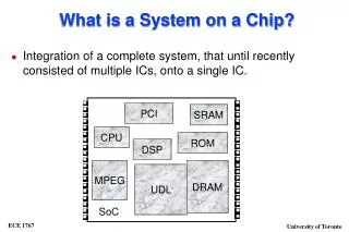
Tile Communication Interface North mProc Multiplier East West ctrl Multiplier FPGA South Core Adaptive System-on-a-Chip (aSoC) • Tiled architecture with mesh interconnect • Point to point communication pipeline • Allows for heterogeneous cores • Differing sizes, clock rates, voltages • Low-overhead core interface for • On-chip bus substitute for streaming applications • Based on static scheduling • Fast and predictable Burleson/UMASS
Communication Interface Core • Custom design to maximize speed and reduce power • Core-ports • Crossbar • Controller • Instruction memory • Local frequency and voltage supply Core-ports North North South South East East West West Outputs Inputs Local Config. Local Frequency & Voltage Decoder Controller Crossbar North to South & East PC Instruction Memory Burleson/UMASS
SoC Infrastructure1,3 Communication Interface Interconnect3 Power Distribution Clock System Power Management Cores Motion estimation for video encoding2,3 AES Cryptography3 Cache2,3 Huffman Coding 3D Graphics1,2,3 Discrete Cosine Transform2,3 Smart Card2,3 Class Projects 1 Used in PhD Dissertation 2 Used in Masters Thesis 3 Used in Publications Burleson/UMASS
Design Flowhttp://vsp2.ecs.umass.edu/vspg/658/TA_Tools/design_flow.html • Architecture to Layout • Architecture: Block diagram of system and behavioral description • Logic: Gate level or schematic description • Circuit: Transistor sizing • Layout: Floorplanning, clock and power distribution • Tools • VerilogXL: behavioral representation • VTVT: standard cell library • Synopsys: standard cell gate level netlist generation • Silicon Ensemble: standard cell netlist to layout • Cadence LayoutPlus: schematic and layout design • NCSU CDK: design and extraction rules • Cadence Layout vs. Schematic: layout verification • HSPICE: circuit simulator Burleson/UMASS
aSoC Implementation and Integration 2500 l .18m TSMC technology Full custom 3000 l Burleson/UMASS
Advanced Signaling Techniques (building on SRC-funded work) Differential current sensing Booster Insertion Multi-level current signaling Phase coding Burleson/UMASS
Circuit Level Simulation (HSPICE)Evaluating Subsystems with realistic models • Capacitance, resistance and inductance • Process variations • Process generations Burleson/UMASS
Interconnect Characterization:Comparing delay and power of signaling techniques for different tile sizes at 250nm, 180nm, 130nm, 100n Burleson/UMASS
Voltage Scaling Approach Core Processing Pipeline • Core-ports • Single buffer for each stream to cross clock/voltage barrier between core and interface • Reading/Writing success rates indicate core utilization • Input blocked: Core too slow • Output blocked: Core too fast • Controller • Interprets core-port success rates to adjust local clock and voltage Local Vdd Local Clock Buffer Input Core-port Output Core-port Clock and Supply Controller Blocked Blocked Interconnect Burleson/UMASS
Vdd Selection Criteria Normalized Core Critical Path Delay vs. Vdd 12 Normalized Delay • As Vdd decreases delay increases exponentially • Use curve to match available clock frequencies to voltages • The voltage and frequency change reduces power by 79%, 96%, and 98.7% • P = aC(Vdd)2f 10 1/8 Speed 8 6 1/4 Speed 4 1/2 Speed 2 Max Speed 0 0.4 0.6 0.8 1 1.2 1.4 1.6 1.8 2 0.73 1.16 Voltage Burleson/UMASS
Clock Distribution Tile • Tiled architecture extends life of globally synchronous systems • Precise H-tree implementation • Load is small and equal at each branch • Skew can be reduced by 70% with advanced deskew circuits1 1 S. Tan et al. “Clock Generation and Distribution for the First IA-64 Microprocessor” IEEE JSSC, Nov. 2000 Burleson/UMASS
Power Distribution • Heterogeneous cores may require multiple power supply voltages • Tile structure enables uniform interwoven grid • Larger grid for higher current demands • Reduced resistance • Higher capacitance Gnd Vml Vl Vmh Vh Burleson/UMASS
Architecture Evaluation(Motion Estimation) Memory • Array-based architecture • Pipelined ME • Parameterized search window size • Full search • Choose 16x16 or 8x8 windows • Reduce power FIFOs Address Generation Unit Processing Element Array Burleson/UMASS
Modify Existing Designs • Take existing Verilog code or hardware and improve or change functionality (e.g. add motion estimation algorithms, provide AES key-length flexibility) • Evaluate changes in performance and overhead - Old PE Layout - New PE Layout Burleson/UMASS
Conclusions • Advancing Process Technology • Target .18u for affordable fab but also do scaling studies • Higher level design tools • Combine synthesis and custom techniques • Realistic yet tractable design projects • Re-use existing projects and provide unifying themes • Preparation for jobs in semiconductor and other sectors. • Focus on system design and appropriate levels of abstraction • Teach how to learn new tools • Making best use of faculty/student time and university resources • Leverage research • Combine grad and undergrad • Re-use materials, tools Burleson/UMASS