Download
1 / 47
560 likes | 1.16k Views
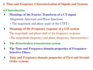
Frequency and Time Synthesis A Tutorial Victor S. Reinhardt June 6, 2000. Frequency and Time Synthesis Tutorial Organization. Basic Concepts What is a Synthesizer? Basic Concepts of Frequency and Time Synthesis Direct Analog Synthesis Analog Building Blocks

E N D
Frequency and Time SynthesisA TutorialVictor S. ReinhardtJune 6, 2000
Frequency and Time SynthesisTutorial Organization • Basic Concepts • What is a Synthesizer? • Basic Concepts of Frequency and Time Synthesis • Direct Analog Synthesis • Analog Building Blocks • (Digital Building Blocks used to Generate Frequencies) • No VCO’s • Indirect Synthesis • Uses Phase or Frequency Locked VCOs • Direct Digital Synthesis • Uses Digital Processing Techniques to Generate Output • Digital Circuits used to Process Numbers • No VCO’s
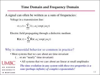
Basic ConceptsWhat is a Synthesizer? One or More Reference Sources fr1 • One or More Input Reference Sources fr1…frn • Translation to NewFrequency fo • Phase or Frequency Coherent With References • Basic Properties • Frequency Range • Frequency Resolution • Switching Rate/Settling Time • DC Power, Weight, Cost, etc. Synthesizer . . . Output fo frN • Phase/Frequency Stability (Time Domain, Environmental Effects) • Spectral Purity (Frequency Domain, Spurs, Noise)
Positive Zero Crossings attn=nTo n=2n V Amplitude A t Sine Wave Period To =2 V Amplitude A t Pulse Ideal Periodic Waveform • Periodic Function F(F) V = A F(F) F = Phase of Function F(F + 2) = F(F) • In Time DomainF = wot wo=Angular Frequency wo= 2pfo fo = 1/To = Frequency • F not a True Observable • Measurement Depends on Inverting F(F) • Must Keep Track of Number of Cycles for Multiples of 2p • Best Determined at Zero Crossings where Slope Large
Non-Ideal Waveform • Amplitude and Frequency Now Function of Time • Angular Frequency Error w w = df/dt • Frequency Error f f =w/2p • Fractional Frequency Error y y = w/wo = df/foy = (df/dt) / wo V Peak VariationAmplitude Error t Zero Crossing VariationTime or Phase Error • Force Nearly-Periodic Waveform into Periodic Form V = ( A + a(t) )·F[ wot + f(t) ] a(t) Amplitude Error f(t) Phase Error
For Sine Wave Near ZeroV = A(wot+f(t)) V F, t dV f, dt Additive Noise and Phase & Time Error • Additive Noise dV Generates Phase Error f(t) = dV(t)/A • fin Radians Equivalent to Noise/Signal Ratio • dB(f) Equivalent to dBc • Time Error in Positive Zero Crossing dt = -f/wo = -dV/(Awo) • Note Minus Sign • PositivedV Negativedt Positivef For Non-Sine Wave: Effective A is Determined by Slope Near Zero Complex Representation dVQ f A dVI dVI = dVQ = dV
Clock Reading vs Time Error Basic Clock • A Basic Clock Contains a Frequency Reference and a Cycle Counter • Zero Crossing Time Errordt = -f/wo • Compares Equivalent Zero Crossings at Different Times • Clock Reading Errorx = f/wo • Compares Cycle Counts or Normalized Phases at Same Time • Note That x = y dtBut dt = - y dt fo Frequency Reference Cycle Counter x x dt Ideal Source
dwo Kdwr dwr yo = = = = yr wo Kwr wr fo Kfr fr xo = = = = xr wo Kwr wr Ideal Coherent Synthesizer • Coherent Frequency Translation by Factor K • Multiplies the Input Frequency fr by a Factor K • Ideal: Doesn’t Add Noise • Input Phase Error fr Also Multiplied by K • The Phase Error Integral of the Angular Frequency Error • The y and x of a Reference Oscillator are Independent of the Final Output Frequency fr fo= Kfr Ideal Coherent Synthesizer fr fo= Kfr Frequency Reference
Important Property of S(f) Filter H(f) V(f) = H(f)U(f) U(f) Sv(f) = |H(f)|2Su(f) dx y(t) = dt df y(t) = wo-1 dt w2 Sy(f) = Sf(f) wo2 Spectral Density Review • A Random Variable u(t) is Wide Sense Stationary if the Autocorrelation Function R is only a Function of tRu(t) = T-1T u(t+t)u(t) dt • The Spectral Density is the Fourier Transform of Ru(t)Su(f) = ej2pftRu(t) dt • For Frequency Translation KSf-output(f) = K2 Sf-input(f) Sy-output(f) = Sy-input(f) Sx-output(f) = Sx-input(f) Sy(f) = w2Sx(f)
Spur Spurs in Time Domain Phasor Diagram • Spurious Signal Rotates around Main Phasor at 2pDf • Time Domain Measurements are Sampled at Multiples oftn = nTo • Generates Regular Pattern at Aliases of 1/Df 2pDf Vo(t) Spur at fo+Df wo f x Discrete Samples When Phasor Crosses Real Axis Phase Error Plot s(t) Allan Variance Counter Histogram t Noise
Mixers fa fa fb fb f f Switches f1 fin f2 fo x fout x . . . . fn Direct Analog Synthesis Multipliers • Directly Generates fo Frequency without VCO • Multiplicative Devices • Multipliers • Dividers • x Conserved • Additive Devices • Mixers • Others • Filters • Switches • Amps • Also Add Their Own Noise x N f Nf f Nf Dividers f f/M ÷ M f f/M x x Filters fb fa+fb+fc f f Amplifiers x x
... f2 f3 f1 Switch Matrix ... 9fr 2fr fr Reference Generator fr Typical Direct Analog Synthesizer: Divide & Mix fo = f1+ f2/10+f3/100 • Two Parts of Synthesizer • Switched Reference Section • Generates References 0, fr,…9fr • Switch Refs to LO’s f1, f2,, f3 … • Divide and Mix Section (3 Stages Shown) • Divide f3=N3fr by 10 • Mix with f2=N2fr and Filter to Produce f2+f3/10 (Bypass Mixer if N2=0) • Repeat Divide, Mix, and Filter with f3=N3fr • End Result fo = [N1+ N2/10+N3/100 + …]fr • Each N Selects Digit of Output fk=Nkfr (Nk = 0 to 9) f1=N1fr + 10 f2+f3/10 f2=N2fr f3/10 + 10 f3=N3fr
S(f) 1/f Noise White Noise Floor 1/f Knee f Si 1-10 KHz GaAs, InP 0.1-1 MHz 1/f Knees Component Design Parameters Phase Noise Characterization of Devices • General Parameters • Frequency Response • Speed (Switches) • DC Power • Cost, Weight, & Size • Phase Noise (See Left) • Phase Stability (Time, Environment) • Filters: Phase Shift over Temperature Critical Issue • Spurs • Mixing IM’s • Switches: On/Of Loss Ratio Determines Spurs • Unwanted Multiplier Orders Cascaded Multipliers & Dividers xN1 xN2 xN3 ÷N3 ÷N2 ÷N1 • These Most Critical for Sf(f) • Make Lowest Noise and Highest N • All x Contributions the Same
Asynchronous Counter FF FF ... FF fin fout Clean-up Circuit fin f’out fout One Shot Synchronous Counter ... fout fin FF FF FF Regenerative Delay-t Divider Set R-S FF Q fin fout Delay t Reset Frequency Dividers (Counters) • Asynchronous (Ripple) • Lowest Power • Most Phase Variation (Cascading Delays) • Can Use Clean-up Circuit • Synchronous • High Power • Lowest Phase Variation • Dual-Modulus • Almost Lowest Power • Low Phase Variation • Limit on Divide Number • Regenerative & Analog Dividers • Can be Very Simple & Low Noise • Limited Frequency Range • Susceptible to Cycle Slips
Dual Modulus Counter ÷ P/P+1 fin ÷ Out P/P+1 Control ÷A Reset A Counter Reset M Counter ÷M fout Dual Modulus Counter • Dual Modulus Counter • High Speed Dual Modulus (÷ P/P+1) Prescaler • 2 Low Speed (÷M, ÷A) Counters • fout = fin/(MP+A) M P, A = 0 to P-1 • Minimum Divide Ratio = P(P-1) • Operation • Prescaler Starts with ÷(P+1) • Prescaler Switches to ÷P when A Count Reached • A and M Counters Reset when M Count Reached (Thus Must Have M A) • Prescaler Switches Back to ÷(P+1) • For Contiguous Divide Numbers A = 0 to P-1 (so Must Have M P-1)
t Frequency Multipliers f Nf Nonlinear Device Filter • 1. Resistive Diode and Mixer • Broadband & Loss • Low Efficiency for High Harmonics • 2. Step Recovery Diode & Varactor • Narrowband (to Match 5 Input Z) • Higher Efficiency for High Harmonics • 3. Transistor • Highest Efficiency (Gain) • Too High Drive Can Cause Slow Damage from Avalanche Breakdown • 2 & 3 Susceptible to Parametric Oscillations Sharpness of DistortionFeatures (t) Determine Amplitude ofHigh Harmonics Good Efficiency Limit Nf 1/t Device Degradation Due to Overdrive
fR fLO fIF Harmonics of fLO Harmonics of fR IF to Spur Ratios (dB) Mixers • Many Types of Mixers • Single Device • Single, Double, Triple Balanced • SubHarmonic (Doubles LO Input) • Single Sideband • Higher Order Mixers Suppress Spurious Mixing Products • fspur = NflO - MfR • (N,M) = Spur Order • Major Issue: Keeping Spurs Away From fIF (WJ-M9E)
Loop Filter fo = T-1(fr) VCO Freq Control Frequency Translation Error Signal Phase or Frequency Discriminator T(fo) fr Indirect Synthesis fo = Nxfr Loop Filter VCO ÷N Error Signal fo/N fr Example: Divider Loop Indirect Synthesis • Utilizes Phase or Frequency Locked VCO to Act as: • Operation Inverter • VCO Output fo Goes Through Frequency Translation T(fo) • Phase or Frequency Discriminator Compares fr to T(fo) and Generates Error Signal • Through Loop Filter and VCO Frequency Control, Error Signal Driven to Zero so fr= T(fo) • Thus VCO Output is Inverse of Tfo= T-1(fr) • Tracking Filter • Uses Bandwidth Properties of Loop to Filter Reference Signal
f = fo- Vo/s Vi = fr- f VCO fr f f Vi G(f) Vo Vo = G(f) Vi H(f) 1-H(f) 1 1 f f fn fn Basic Phase Locked Loop • Definitions • Open Loop Gain G(f) • Output Phase Error f • Reference Phase Error fr • VCO (Free Running) Phase Error fo • Closed Loop Response H(f) = f/fr = G(f)/(s + G(f)) • H(f) has Low Pass Response with Knee at fn • 1-H(f) has High Pass Response with Knee at fn • Output Phase Error f = H(f)fr + (1-H(f))fo • Reference Characteristic f << fn • VCO Characteristic f >> fn Idealized PLL
Sf(f) Free Running VCO Sf(f) Reference Sf(f) Optimum PLL Sf(f) f Optimum fn Optimum Loop Bandwidth • Free Running VCO: • Higher Near In Noise • Lower White Noise Floor • Reference • Lower Near In Noise • Higher White Noise Floor • Optimum Loop Bandwidth fn for Integrated Noise is Where Curves Cross • May Have Other Reasons not to Choose this fn Such as Settling Time Requirement
Oscillator Noise Characteristics Loss = L Resonator • Simple Oscillator Model • Amp NoiseSa(f) = (FkT/Pin)·(1 + ff/f) • Leeson’s Equation • Net Phase Around Loop = 0 fR = -fa= -2QL·y • Note Resonator fR vs y slope Controls Oscillator Frequency • Thus Amp Phase Noise is Converted to Oscillator Frequency Noise Sy(f)= 1/(2QL)2Sa(f) • Since Sy(f) = (f2/fo2)Sf(f) We Obtain Leeson’s Equation Sf(f) = (fo/(2QLf))2+1)(FkT/Pin)(1+ ff/f) Loaded Q = QL Near Resonance fR = -2QL·y Oscillation Conditions |GaL| = Loop Gain > 1 Sf Around Loop = 0 Pin Amp Gain = Ga Noise Figure = F Flicker Knee = ff Noise Density = FkT Converted Noise + Original Amp Noise
Sf(f) K3/f3 Converted Noise QL K2/f2 Amp Noise K1/f K0 f Oscillator Noise Spectrum Oscillator Noise Spectrum • Oscillator Noise Spectrum • Sf(f) = K3/f3 + K2/f2 + K1/f + K0 • Some Components May Mask Others • Converted Noise • K3/f3and K2/f2 • Varies with (fo/(2QL)2and FkT/Pin • Amp Noise • K1/f and Ko • Only Function of FkT/Pin Leeson’s Equation Sf(f) = (fo/(2QLf))2+1)(FkT/Pin)(1+ ff/f)
Multiplied Oscillator Sf(f) xN Nfo fo N2 N2 f Sf(f) = N2(fo/(2QLf))2+1)(FkT/Pin)(1+ ff/f) Oscillator at fovs Nfo(Same QL) Sf(f) vs fo Nfo N2 Sf(f) = (Nfo/(2QLf))2+1)(FkT/Pin)(1+ ff/f) Multiplied Oscillator vs Higher Oscillator Frequency • Multiplied Oscillator • Whole Curve xN2 • Higher Near-in Noise • Higher Far-out Noise • Oscillator foNfo • Only Converted Noise xN2 (Same QL) • Higher Near-in Noise • Same Far-out Noise (Same FkT/Pin) • This is Why Indirect Synthesis is Attractive • For Lower VCO QL than Ref QL Bump in Curve
Classification of Loops • Loop Order (1st, 2nd, etc.) • Phase vs Frequency Lock • PLL Lower Near in Phase Noise • PLL: Loop Noise Converted to White Phase Noise • FLL: Loop Noise Converted to White Frequency Noise • FLL Settles Faster • Implementation • Analog Loops • Analog Phase Discriminator • Digital Phase Discriminator • Digital Loop (Filter) • Phase/Frequency Error Quantization • Contininuous (or Near Continuous) • Bang-Bang (Sign of Error)
Damping Factor z = wn 2szwn+wn2 H = H = s + wn s2+2szwn+wn2 1st & 2nd Order PLLs 1st Order PLL 2nd Order PLL • DC Open Loop Gain Set by wn (= 2pfn) • VCO Drift will Eventually Cause Loop to Unlock • Doesn’t Completely Suppress Near-in VCO Noise (1/f3) • Fastest Settling Time for Same wn • Injection Locked Oscillators equivalent to 1st Order PLL fr f fr f VCO VCO wn = G 1-H = s for s << wn 1-H = s2 for s << wn • DC Open Loop Gain Virtually Infinite • VCO Drift No Problem • Completely Suppresses Near-in VCO Noise (1/f3) • Slower Settling Time for Same wn
Analog (Loop Filter) PLLs fo VCO • Phase Detectors • Mixers - Need Locking Circuit • Phase-Frequency Det. - Self-Locking • Loops with PFDs Also Called “Digital” Loops • Divider Loop • Easy Lock • ASIC Implementation with PFD • Mixer & Loop Noise xN • Multiplier Loop • False Lock & Spur Issues • Mixer & Loop Noise Not Multiplied • Sampling Phase Detector This Type • Can Also Have Multiple Conversions (Mixers) Analog Loop Filter Analog Frequency Translation Voltage Output Phase Detector fr Divider Loop fo/N fo fr ÷N Multiplier Loop frxN fo fr xN
fr1 . . frk Digital (Loop Filter) PLLs Digital Loop Filter fo VCO D/A • Can Lock to Many fr’s: fr1 ... frk • Weighted Averages, Separate Frequency Offsets, Error Correction • Digital Phase Detection • Mix each frkto Lower fIFk = K(frk-K’fo) • Counters Measure Zero Crossings tnk of fIFk with Resolution 1/fc • Used to Calculate fIFk =K(frk-K’fvco) • Single Measurement Resolution df = 2pfIF /fcMust be < RefNoise to Avoid Spurs • Digital Loop Filter & D/A Control VCO • Loop Filter Sampled at Rate fIF • D/A LSB Must be < Ref Noise in Time 1/fIF to Avoid Spurs (Note: Frequency Resolution is Not Set by D/A LSB) Analog Down- Conversions Averaging .. fIF1 fIFk Digital Frequency Translations Counters fc from VCO TIF = 1/fIF tnk Tc = 1/fc fIFk = 2p ( n - fIFk tnk ) df = 2p Tc / TIF = 2p fIF / fc
10.23 MHz VCXO VCXO AFS fo fo fr1 fIF1 Down- Converter AFS 1 D/A 3.17 MHz 13.4 MHz AFS’s 100 Hz 4 Event Clock & PLL Processor fr2 Down- Converter AFS 2 180 KHz fIF2 76 Event Clock & PLL Processor 3.53 KHz Cs 2.76 KHz Rb 10.23 MHz from VCXO 98 ns Event Clock From D/C x 2n N + + 2nd Order Loop Filter To D/A N= 3800 Cs N= 4858 Rb - - Compute Phase Integrate x n2/s ~100 Hz Integrate Downconverter f Offset f Offset Example of Digital PLL (Reinhardt, 1999)
Ping Pong Switch fo 2nd PLL Pre- tune ÷N Adaptive Loop Filter fr Pre- Charge Reclock & Clear Divider Fast Settling Loop Techniques • Pretune VCO Voltage • Approximate New Frequency • Precharge Loop Integrator • Preset for New VCO Frequency • Adaptive Loop Filter • Dynamically Adjust Bandwidth • Reclock & Clear Divider • When Frequency Changes, Old Nozero State is Phase Error that Must be Slewed Out in PLL • Reclocking and Clearing Eliminates this Phase Slew • Ping-Pong Switch & Second PLL • Presettle 2nd PLL before Switching
Effect of Precharge on Transient Response • Precharge Pre-loads Integrator at Each New Frequency Command • Generates More Ideal Stepped Frequency Response Loop TC = 0.1 s (Reinhardt, 1999)
Cycle Slipping Mechanical Model of PLL with Noise • Becomes Problem at Low SNR within the Loop BW • Phase Detectors are Periodic in Phase • Finite Probability of Noise Burst Large Enough to Cause Slip to Next Cycle • Mean Time to Cycle Slip Exponential Function of 1/SNR in Loop BW • Especially Problem with Sampling Phase Detectors Noise Burst Causes Cycle Slip Average Noise Energy f (Kroupa, 1973)
Post-Tuning Drift Response to Voltage Step • Post-Tuning Drift is Further Settling of VCO Frequency After Main Exponential • Can Last s to Hours • Can Have Multiple time Constants • Causes • Thermal Effects in Semiconductors • Surface Charging and Traps in Semiconductors • Bias Circuits and Regulators • Problems/Issues • Varactor Tuner Prime Source • GaAs Devices are Especially Prone to Post-Tuning Drift • Semiconductor Effects are Very Lot Dependent Post-Tuning Drift VCO Frequuency Single Exponential Equivalent Circuit of a Diffusion Process
Direct Digital Synthesizers • DDSs also called Numerically Controlled Oscillators • Directly Synthesize a Selectable Output Frequency from a Clock Using Digital Techniques • Types of DDSs • Pulse Output • Sine Output • Fractional Divider • Fractional Divider Phase Interpolation • Other
R Carry Carry Timing Jitter Carry Clock Cycles Tc 1 2 3 4 5 6 7 8 9 Pulse Out Pulse Output DDS Accumulator Used as DDS • DDS is N-Bit Accumulator • For Each Clock Period 1/fc Rin + K Rout in N-bit arithmetic • Can Write as Frac(rin + F) rout • Fractional Frequency Word F = K/2N • Fractional Register Value r = R/2N • Carry (or MSB) Output • On Average fo = F fc • RMS Jitter (No Output Filter) • Period Jitter Tc/(12)0.5 • Phase Jitter pF/(3)0.5 • Example F=3/8, (To=(8/3)Tc) • r = 0(C), 3/8, 6/8, 1/8(C), 4/8, 7/8, 2/8(C), 5/8, 0(C), ….. • Period Errors (dT/To): 1/3, 1/3, -2/3 fo Frequency Word K Pulse Out N-Bit Adder A Carry N-Bit Register Rout B A+B fc Rin “Square” Wave Out MSB Clock
Typical Pulse Output DDSFrequency Spectrum • Large Spurs Very Close to Carrier • Nature of Spurs Changes Drastically with fo • Filtering Doesn’t Necessarily Reduce Phase Jitter (When Nearby Spurs Present) • In General Closest Spur 2-Nfc f = 0 . 1 2 2 5 H z f = 1 H z o c 0 Carrier -20 -40 -60 -80 0 0.2 0.4 0.6 0.8 1.0 F r e q u e n c y ( H z )
W Bits fc Sine Table N-Bit Accumulator K J-Bits fo Filter DAC M-Bits Sine Output DDS • Reduces Spurs by Adding Sine Table and DAC • N Determines Frequency Resolution • Argument of Sine Table = W Bits out of N Bit Accumulator • Sine Table Value = J Bits • DAC M Bits • Nyquist Theorem: No (In-Band) Spurs if • Sine Table and DAC Perfect • fo < 0.5 fc (Must LP Filter Output) • Spur Levels • 6 dBc per bit for W & J • 6-8 dBc per bit for M (Use Effective Number of Bits not Actual Bits) • Worst Case Determines Spurs Stepped DDS Output
5-Bit DAC 11-Bit DAC 0 -10 -20 -30 -40 -50 -60 -70 -80 -90 dBc fo=333.25 KHz fc=1 MHz Span=10 KHz RBW=10 Hz Typical Sine Output DDSFrequency Spectrums
Spurious/Harmonics STEL-2373,[1] Raytheon [2] -19 Plessey(4) SP2002,[3] -29 Rockwell,[4] -39 TI / Lincon Labs LDDS,[5] Sciteq DCP-1A,[7] -49 Sciteq ADS-43x[7] -59 Sciteq (5) ADS-63x [7] -69 Hughes Space[8],[9] -79 Philips Microwave Limeil,Thomson CNI[10] 25 125 333 190 245 295 450 TRW DDS/HDAC-1,[11] 0.29 DAC Triquent SC-0806- C,(1)[21] High Speed DACsSpur Levels vs Speed dBc Output Frequency (MHz) (Essenwanger & Reinhardt, 1998)
None 214x12 1:1 (none) -97.23 Modified 28x9 Unmodified Sunderland 28x11 12-bits ±2 LSB 59:1 51:1 adder adder -86.91 Sunderland 28x4 28x4 28x9 Nicholas 128:1 adder/subtract -88.94 28x3 27x14 Conventional Taylor Series 2 adders multiplier 64:1 -97.04 27x9 25x3 14 pipelined stages 18 Bits Wide Cordic (none) N/A -84.25 27x14 Raytheon Taylor Series multiplier multiplexer, adder 13-bits ±1 LSB 27x11 67:1 25x7 3 pipelined stages Requires 1 calc of Sinf & Cosf per Freq IIR Filter* (Presti, et. Al.) (none) N/A No Limit Sine Table CompressionAlgorithms Compression Algorithm ROM Req’ed Compression Ratio Logic Circuits Algorithm Error (dBc) (*Modified from Essenwanger & Reinhardt, 1998)
R Carry Carry Clock Cycles Fractional Divider or Pulse Swallowing DDS • Dual Modulus Prescaler • Normally ÷ n • Output Clocks Accumulator • On Accumulator Carry ÷ (n+1) Next Cycle • N-Bit Accumulator R + K R • Carry on Overflow • Output on Prescaler • On Average fo = fc/(n+F) • RMS Jitter (No Output Filter) • Period Jitter Tc/(12)0.5 • Phase Jitter p/(n+F)(3)0.5) fc fo K Dual Modulus Prescaler ÷n/n+1 N-Bit Accumulator Carry ÷n/n+1 Control
fr Linear Phase Detector K R DAC N-Bit Accumulator Loop Amp Carry Output n/n+1 Control fo VCO Divide by n/n+1 Phase Interpolation Fractional Divider (in PLL) • Fractional Dividers Utilized Most Often in PLLs • Can Reduce Phase Jitter by Utilizing R Value • At Carry rTc = Period Error • Utilize DAC & Linear Phase Detector to Correct for Error Represented by R • Spur Levels Limited by • Linearity of Phase Detector • DAC Resolution • Without Interpolation Can Reduce Spurs if 2-Nfc >>Loop Bandwidth
Spur Generation in DDSs Accumulator Samples v(r) at rn=fotn Stepped Output Hold Function Look-Up Table v(r) • Quantized Sine Wave (Sine DDS) • Square Wave (Pulse DDS) • v(r) Periodic in r (Period=1) • Discrete r-Space Harmonics • Stepping Adds Hold-Function Filter • Spectrum of Hold Function Sinc2(f/fc) • v(fot) Translates mth Harmonic to mfo • Sampling at tn Causes Aliasing at f=mfo - m’fc t-Space Sampled Spectrum Output Spectrum r-Space Spectrum Harmonics 1 1 3 3 5 5 7 7 1 3 5 7 r-Space Frequency 0 0 fo 2fc fc 2fc
DDS Spur Algebra • Time Domain Properties of rn = Frac(nF) • Produces Periodic Sequence • In Irreducible form F can be Written as a/b (a and b Relatively Prime) • Time Domain Sequence Permutation of 0, 1/b, 2/b, …. (b-1)/b • So Period of Sequence bTcand Number of Unique Values b • Frequency Domain Properties • Since Period bTc Sequence has Harmonic Exdpansion kfc/b = 0, fc/b, 2 fc /b, …. (b-1) fc /b, .... kfc/b = mfo - m’fc = [m(a/b) - m’]fc • Thus • There are b Spurs from 0 to fc • The Spur Spacing is fc/b • There is a Large (Principal) Spur at fc-fo that is an Alias of the (Negative) Fundamental Frequency
r r + p v(r + p) N-Bit Accumulator v(r) Random Number Generator Fractional Frequency F p Destroying Coherence With Register Jitter • Spurs Occur Because Uniformly Stepped Sequences Periodic • Introducing Jitter Destroys Periodicity • Jitter More Efficient with Spurs from High Harmonics of v(r) Expansion • Converts Spur Energy to Broadband Phase Noise Heuristic Explanation Spur Height Reduced Because of Larger Jitter S(f) Jitters Output at fo by Jitters spur from mth Harmonic of v(r) by m fo fspur f Converts Spurs to Broadband Spectrum
Wheatley Jitter Injection f = 0 . 1 2 2 5 H z f = 1 H z f = 0 . 1 2 2 5 H z f = 1 H z o o c c • Used with Pulse Output DDS • Destroys Spurs but Produces High Degree of Broadband Noise 0 0 Carrier Carrier -20 -20 -40 -40 -60 -60 -80 -80 0 0.2 0.4 0.6 0.8 1.0 0 0.2 0.4 0.6 0.8 1.0 F r e q u e n c y ( H z ) Without Jitter Injection With Jitter Injection
0 0 -10 -10 -20 -20 -30 -30 -40 -40 -50 -50 -60 -60 -70 -70 -80 -80 -90 -90 dBc dBc Randomized DAC DDS Experimental Results 5-Bit DAC No Jitter 5-Bit DAC With Jitter 11-Bit DAC No Jitter • Used with Sine Output DDS • Less Efficient at Reducing Spurs but with Lower Broadband Noise fo=333.25 KHz fc=1 MHz Span=10 KHz RBW=10 Hz (Reinhardt,1993)
Frequency and Time SynthesisFinal Summary • The Basic Concepts Basic Outlined Here are Provide a Framework for Both the Design & Specification of Frequency and Time Synthesizers • The 3 Types of Approaches Outlined Here Are • Analog Synthesis • Indirect Synthesis • Direct Digital Synthesis • The Above Architectures Used in Combination are Often the Best Design Approach • A List of References Follows