Download

1 / 28
280 likes | 385 Views
Understand and classify faults in FPGA bitstream to enhance system reliability in radiation-prone environments. Emulation method for fault analysis. Test all vulnerable bits.

E N D
Emulation of SEU Effect In Bitstream of FPGA Jiří Kvasnička, Hana Kubátová
Introduction to SEU • FPGA devices are widely used IC in many target application • SEU (Single Event Upset) is an undesirable effect caused by charged particle, that can modify the design by reversing 1 bit in configuration memory SEU represents a problem: • For SRAM memory (configuration memory, registers, distributed RAM) • especially in radiation hostile environments (airplanes, satellites) and nuclear facilities (nuclear plants, colliders) • even in devices operating at sea level (290FIT/Mb @ Xilinx Rosetta experiment; FIT = failure per 109hours) • Dependability of a system built on SRAM based FPGAs depends on a mapped, placed and routeddesign [Aerospace corp.]
[Aerospace corp.] How to estimate FPGA design reliability? • Irradiation by a particle beam • most exact results • expensive, labor-intensive • results from mapped and routeddesign loaded in FPGA • Software simulation • is possible only with FPGA layout knowledge (therefore is limited only to manufacturers): • without FPGA layout knowledge: limited to RTL level • Emulation in hardware • SEU is emulated by a bit-flip in bitstream • results from mapped and routed design loaded in FPGA • FPGA layout knowledge helps in results interpretation
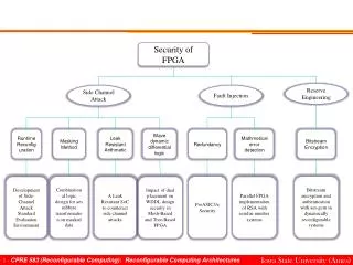
FPGA structure classification • Bits of FPSLIC bitstream can be classified into following groups, according to a function of bits: • LUT • Cell interconnection • Cell to BUS connection • BUS crossing • BUS repeater • Unexplored (includes: clock, reset, distributed RAM) • I/O (untested) • “Other” (glue bitstream bits without function)
FPGA Fault classification • Each bit can be classified by its fault model • Categories are designed exclusively to FPSLIC • Association with fault model depends on the mapped design • 3 main groups: • Used (bits related to the design) • Unused (outside the design) • Unknown (unexplored) (not decided weather Used/Unused, due to limited bitstream knowledge)
Faults in FPGA (1/3) • Unused • “don’t care” bits • Bits in this group do not lay in the design area • Can not affect the design • Antenna • An unused wire is connected to the data-path • Has no static influence on the design • extra load capacitance delays can worse
Faults in FPGA (2/3) • Alternate • These bits alternate the design • No conflict is caused by alternate • Open • these bits cause data-path to break
Faults in FPGA (3/3) • Conflict • Occurs when 2 driven wires are connected • “0-F” between constant 0 and any function • “F-F” between 2 function • Unpredictable • special case of open, where the default logical value “1” is substituted with “Z”
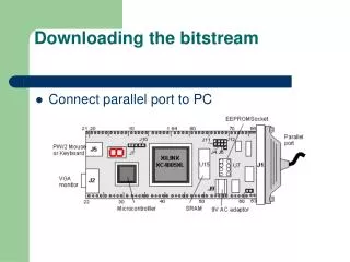
Emulation of FPGA faults • AT94K40AL FPSLIC (FPGA+AVR) • SEU is emulated by a reconfiguration of 1 bit of configuration memory • 2 copies of benchmark present: “tested” and “golden” reference copy • VR controls the testing and reconfiguration • Bitstream analysis and set of bits selection are performed in PC.
Summary: Obtaining reliability of the design • Step 1: synthesize, place and route the design • More exact result from mapped design • Step 2: analyze each bit of the bitstream • Separate bits, that do not harm the design • Rough estimation • Analysis significantly reduces set of tested bits • Step 3: test all possible vulnerable bits (short, open, conflicts, alternates…) Results follow on next slides…
Conclusions + Well-proven design flow for benchmark testing + Bitstream test coverage 95.5% + Fast selection and separation of vulnerable bits (at O(n) time complexity) ± Results are affected by place and route process – FPGA structure and bitstream knowledge is required for correct area and fault classification and for exact vulnerable bit selection – Advantage of testing speedup (with comparison with software simulation) is degraded by time needed for Place&route and programming
Fault injection • MD4 bitstream format is used • It consist of 4 byte register: • Z value represents a “layer”, which selects a type of FPGA resource • X and Y values are related to location of selected resource • D contains up to 8 bits of bitstream • A new configuration byte is created by changing bit in a configuration byte
Bitstream analysis and visualization • s1488 benchmark shown on example figures • All bits from the left half of the FPSLIC device are selected • Analysis is based on wire driving state observation and possible fault determination
Detailed fault effect classification • A: Hidden fault(The result is always OK) • B: Detected fault (wrong result always detected by CED) • C: Undetected fault (result is wrong, but never detected by CED) • D: Temporarily detected fault (The wrong result is sometimes detected by CED and sometimes is not) • Possibility of further Fault security(A or B), Self Testing(B or D) and Totally Self-checking(B) parameters computation
FPGA structure – areas All bits Vulnerable bits of s1488 benchmark
[Aerospace corp.] [Aerospace corp.] How to estimate reliability? • Irradiation by a beam of particles • most exact results • expensive, labor-intensive • results from mapped and routeddesign loaded in FPGA • Software simulation • is possible only with FPGA layout knowledge (therefore is limited only to manufacturers): • without FPGA layout knowledge: limited to RTL level • Emulation • SEU is emulated by a bit-flip in bitstream • results from mapped and routed design loaded in FPGA
FPGA Emulator key features • Observe the SEU resistance of the design mapped in FPGA (with regard to the bitstream utilization) • The SEU is emulated by 1-bit change in the bitstream • Evaluation of Fault Security (FS), Self Testing (ST) and Totally Self-Checking (TSC) properties • Evaluation of dependability parameters for practical application