Download
1 / 60
610 likes | 799 Views
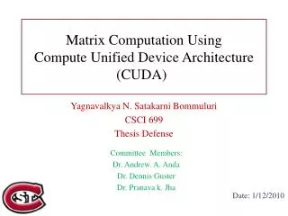
Matrix Computation Using Compute Unified Device Architecture (CUDA) ). Yagnavalkya N. Satakarni Bommuluri CSCI 699 Thesis Defense. Committee Members: Dr. Andrew. A. Anda Dr. Dennis G uster Dr. Pranava k. Jha. Date: 1/12/2010. OUTLINE. Brief Review of the Literature.

E N D
Matrix Computation UsingCompute Unified Device Architecture (CUDA)) Yagnavalkya N. Satakarni Bommuluri CSCI 699 Thesis Defense Committee Members: Dr. Andrew. A. Anda Dr. Dennis Guster Dr. Pranava k. Jha Date: 1/12/2010
Evolution of Computer Architecture Von Neumann Architecture Stored-program concept. Single instruction stream. Single system bus. Harvard Architecture 1) Physically separated storage and signal pathways for instructions and data. Central processing Unit Arithmetic- Logic Unit I/O Equipment Main Memory Program Control Unit Apercus Structure of the IAS Computer
Evolution of Computer Architecture Limitation : Speed of the light Solution: Parallelism Consequence: Parallelism is opted in various forms at different levels to the Von Neumann architecture Legends: I/E: Instruction Fetch and Execute ILP: Instruction Level Parallelism MFU: Multiple Functional Unit RISC: Reduced Instruction Set Computer VLIW: Very Long Instruction Word
Evolution of Computer Architecture Classification of computer architectures based on Flynn’s Classical Taxonomy
Evolution of Computer Architecture Vector Processors • Vector processors are the coprocessors that operate on a linear array of operands called vectors using a single instruction • In the early 1970s vectors architectures are considered as favorable choice for building supercomputers. • The golden era of vectors supercomputers was not until the introduction of CRAY – 1 in the year 1976. • Advancements in CMOS VLSI technology improved the performance the low-cost commodity microprocessors. • In the early nineties, the high cost of vector supercomputers diminished their popularity.
On-CPU Graphics Advancements(FMA, MMX, SSE) • A CPU is a general purpose processor for performing various arithmetic, logical and control operations. • It is not exclusively built for performing graphics related applications, although it includes certain limited features such as FMA, MMX, SSE etc., that support vector and/or graphics applications • A system architecture that is designed for the graphics related applications off-CPU is referred as a GPU.
On-CPU Graphics Advancements- FMA • A “Fused multiply-add (FMA)” is a compound floating-point operation that computes scalar affine operation (x * y) + z to an infinite precision, and rounds once to the result format.
On-CPU Graphics Advancements- FMA • Motivation - Accuracy Enhancement • Floating-point arithmetic operations are unfaithful • Higham has analyzed various summation methods for floating point numbers, and concluded with a remark that no method guarantees the accuracy in the floating point summation [HIGH93 ]. • The inaccuracies are quite ordinary, in the computation of scalar affine operations of the type f(x,y;z) := ((x * y) ± z • High precision software (such as LBNL quad-double precision) can result in greater accuracy but has performance issues due to overheads. • Therefore, in order to enhance the accuracy along with speed of the floating-point computations, manufactures are beginning to provide reliable rounding affine operation called fused multiply-add (fma)
On-CPU Graphics Advancements- FMA Downside • IEEE standard has neither anticipated nor recommended the FMA instructions. Why? • Inconsistent results (x + iy)*(x - iy) = x2 + y2 + i(xy - yx) • Nonmonotonicity If (a * b) – (c * d) ≥ 0, then a * b ≥ c * d, whence fl(a * b) ≥ fl(c * d) • In conclusion, although fused multiply-add can maximize the performance, it may advice not be inhibited to write the programs due to its undesirable effects [HIGH02, p47].
On-CPU Graphics Advancements– MMX MMX Technology - Introduction • The Intel MMX technology comprises a set of extensions to the Intel Architecture (IA) that are designed to accelerate multimedia and communication applications. • Backward compatibility with previous versions of software and operating systems • New extensions: • Eight MMX 64-bit registers (MM0 through MM7) (aliased with FPU data register stack ) • Four MMX 64-bit data types • The MMX instruction set consists of 57 new instructions
On-CPU Graphics Advancements– MMX • Not to endow the 64-bit capability to the Pentium processors • Instead, MMX 64-bit technology uses the single instruction, multiple data technique for performing arithmetic and logical operations on the bytes, words, or doublewords packed into 64-bit MMX registers. • Speeds up the software performance MMX Technology - Motivation
On-CPU Graphics Advancements– MMX Downside - MMX Register Aliasing • MMX Technology is compatible with IA technology. How is this made possible? • It is possible by aliasing MMX registers and state upon the IA floating-point registers and state. • So once a MMX instruction has start executing, another FPU instruction execution is not possible until EMMS is executed. • Moreover, MMX architecture works only on Integer data types.
On-CPU Graphics Advancements– SSE Streaming SIMD Extension (SSE) Technology • To greatly enhance the performance of advanced media and communications applications. • To address the pitfalls of Intel MMX tech. • New Extensions: • Eight SIMD floating-point registers (XMM0 through XMM7). • SSE data type is a packed, four 32-bit single-precision (SP), floating-point number • The SSE exploits the SIMD technique to perform ALU operation on the single-precision; floating-point values in the 128-bit SIMD floating-point registers. [IEEE 754 ]
On-CPU Graphics Advancements– SSE2 Second iteration: Intel SSE2 • Improves the capabilities of both MMX and SSE instruction set • New Extensions: • Additional 144 instruction. • MMX technology have been extended from 64 to 128 bits • Double-precision (64-bit)floating point SIMD instructions support to SSE technology • Enhancement to the original SSE instruction to support arithmetic operations on multiple data types (e.g., double words and quad words).
On-CPU Graphics Advancements– SSE3 Third iteration: Intel SSE3 • In 2004, Intel has further extended the SSE2 technologies to create SSE3. • New Extensions: • Packed horizontal add instructions that operates horizontally on the data registers . • Support for Hyper-Threading (HT) Technology • Prescott New Instructions (PNI) including instruction to convert floating-point values to integers without changing the global rounding mode . • Deeper pipelining to enable higher frequency . • Useful in areas like complex algorithms and video decoding.
On-CPU Graphics Advancements– SSSE3 Fourth iteration: Intel SSSE3 • Supplemental Streaming SIMD Extension 3 (SSSE3). • 16 new discrete instructions over SSE3 • Each can act on 64-bit MMX or 128-bit XMM registers
On-CPU Graphics Advancements– SSE4 Fifth iteration: Intel SSE4 • Released in September, 2007 • SSE4 is the largest Instruction Set Architecture (ISA) extension with respect to capacity and impact since SSE2. • SSE4 has several compiler vectorization primitives along with new and innovative string processing instructions. • 54 new instructions. • Lacks support operations on 64-bit MMX registers. • Supports 128-bit XMM registers only.
On-CPU Graphics Advancements– SSE5 AMD SSE5 • Announced by AMD on August 30, 2007 • 170 new instructions with greater benefits in domains like HPC, multimedia, and security applications than previously released SSE instruction sets. • It is not a superset of SSE4 but a competitor to it • The new instructions include • Fused multiply accumulate (FMACxx) instructions • Integer multiply accumulate (PMAC, PMADC) instructions • Permutation and conditional move instructions • Vector compare and test instructions • Precision control, rounding, and conversion instructions
Memory Controller MEMORY G P U HOST Interface C P U PCI - E Graphics Processing Unit (GPU) – Introduction • A GPU is a single chip processor that can render 2D and 3D graphics. • Technically, a GPU involves the execution of graphics pipeline to render 3D graphics. • Graphics Processing Unit (GPU) act as coprocessor to CPU • Off-CPU Graphics Advancements - GPU
Graphics Processing Unit (GPU) – History Off-CPU Graphics Advancements - GPU
Graphics Processing Unit (GPU) – History Off-CPU Graphics Advancements - GPU
Difference – CPU & GPU • Over the last decade GPUs are getting faster rapidly with tremendous memory and computation horsepower . • The GPUs have grown exponentially at a rate far estimated by Moore’s law. • Why not same with CPU? - same fabrication tech., • Difference is with how the transistors are employed? • Off-CPU Graphics Advancements - GPU GPU CPU
The term General-Purpose Computation on GPU (GPGPU) refers to the computation on graphics hardware for non-graphics applications. • The GPGPU community of developers and researchers (http://www.gpgpu.org/) has started their early ground work of exploiting graphics hardware resources for non-graphics applications. • Why we need GPGPU? • Multiple Programmable shaders • Powerful (Memory Bandwidth, Computational Horsepower (GFLOPS)) • Accuracy • Affordable • Less Power Consumption • GPGPU
Graphics API Programming Model • Graphics API languages like Open GL, Direct3D. • Need CPU-GPU domain correlations. • Adding two numbers procedure : • GPGPU
CPU APPLICATION CUDA Libraries CUDA Runtime CUDA Drivers GPU NVIDIA CUDA • Compute Unified Device Architecture (CUDA). • Anovel hardware architecture and software for issuing and managing computations on the GPU as a massive data-parallel computing device. • Does not require mapping CPU computational concepts. • CUDA uses a C-like language with minimal extensions for general purpose computation on GPU. • GeForce 8 Series, Quadro FX 5600/4600, and Tesla solutions. • GPGPU
CUDA – Shared Memory • Enables General Read and Write Access of Data by Threads • Brings Data Closer To ALUs • GPGPU
CUDA – Programming Model • GPGPU Func<<< Dg, Db, Ns >>(parameter);
CUDA – Memory Model • GPGPU
CUDA – Hardware Model • GPGPU
CUDA – Restriction • Threads and thread blocks can be created only by launching a parallel kernel, not from within a parallel kernel. • CUDA requires that thread blocks be independent as communication between thread blocks within the same grid of blocks is not allowed. • CUDA allows blocks to be executed in any order. The results computed by multiple blocks are combined by invoking a second kernel. • Recursive functions are not allowed in the CUDA. • The overhead of CPU-GPU coordination and data transfers can reduce the overall performance of the CUDA-enabled application. • GPGPU
Basic Linear Algebra Subprograms (BLAS) • API standard for publishing libraries to perform basic linear algebra operations such as vector and matrix multiplication. • Originally implemented in Fortran. • C interface also available (referred as cblas) • Not to confuse with BLACS. • BLAS Levels: • BLAS
NetlibBLAS • Netlib contains the repository of implementation of BLAS complied for various operating systems and hardware. • Also known as generic BLAS. • Not considered as optimized BLAS. • High Performance Non-vendor BLAS • Automatically Tuned Linear Algebra Software (ATLAS), Goto BLAS and μBLAS. • More efficient than generic Netlib BLAS. • Ideal for the new system architecture or to the systems that don’t have their architecture-specific often vendor-specific BLAS. • Vendor-specific BLAS • Built exclusively for specific hardware architecture. • Usually efficient that Non-vendor BLAS. • BLAS
Vendor-specific BLAS • BLAS
Given a square matrix A of Cn X mand a vector v of Cn. • The order-m Krylov subspace is defined as the linear subspace spanned by the base vectors of v under the first m powers of A. • Assuming A0 = I, an order-m Krylov subspace denoted by Km can be equated to a subspace span as shown below: • All algorithms that work this way or use Krylov subspace span as their foundation are called Krylov subspace methods • Krylov Subspace
Motivation for the Study • The purpose of this thesis is to study the performance enhancement of dense matrix and vector computations on a GPU using CUDA. • Immediate benefits for the scientific computation, engineering and high performance numerical computation (HPNC). • Intend to study the impact on performance by implementing certain Level-1, Level-2 and Level-3 BLAS routines on Tesla C870 processor board (GPU) using CUBLAS 2.0 and on 2.3 GHz Quad-core AMD Phenom processor (CPU) using Intel MKL 10.1. • Furthermore, to understand the reusability of data on CUDA, we also computed Krylov subspace for various orders of matrices and base vectors by implementing Level-2 BLAS iterations.
The CUDA programming model utilizes similar performance efficiencies, as related to models for programming on graphics hardware. • The CUBLAS 2.0 and Intel MKL 10.1 BLAS are the efficient (in exploiting the hierarchal hardware architecture), optimized, and threaded BLAS implemented for GPU and CPU architecture, respectively. • The CUDA programming model is a scalable and efficient general purpose computation on a GPU. • Assumptions
We will only include the practical implementation of CUDA programming model, using CUBLAS, and the CPU model, using Intel MKL BLAS. • We do not include other GPU programming models due to lack of testing facilities. • We include the implementation of SGEMM (BLAS Level -3), SGEMV (BLAS Level -2), SDOT (BLAS Level -1) and SAXPY (BLAS Level -1). Furthermore, we will find Krylov subspace of various orders using Level-2 BLAS routines. The implementation of other BLAS and/or algorithms is not included. • Constraints
Under which contexts can CUDA outperform the CPU model for dense matrix computations? • Is CUDA a scalable and efficient parallel programming model? • Hypotheses Questions
Hardware Description • Methodology
Software Description • Methodology
BLAS Implemented • Additionally, computed Krylov subspace using level-2 BLAS. • Methodology
Install Windows Vista Business 64-bit Edition. • For Intel MKL BLAS implementation • Install Microsoft Visual Studio 2008 (MSVS 2008) Pro Edition. • Install Intel Math Kernel Library . • Link the program with Intel® MKL from the Microsoft Visual C++. • Create, build and run program(s). • For CUBLAS implementation • Install Tesla C870 processor board as per the manual. • Install CUDA Toolkit, SDK, drivers version 2.0 for Vista 64-bit. • Install Microsoft Visual Studio 2005 (MSVS 2005) Pro Edition. • Create a new CUDA project from template. Set the “Configuration Manager” to x64 platform. Build and execute the application on x64 bit mode. • Methodology
The following three variables are measured in each experiment for various sizes of square matrices and/or vectors using clock_t clock(void) function available in the header file <time.h>. • The Intel MKL BLAS computation time in milliseconds. • The CUBLAS computation time is measured as the number of clock ticks elapsed for the execution of the CUBLAS kernel on the GPU device. • CUBLAS total time = host to GPU data transfer time + CUBLAS computation time + GPU to host data transfer time. • Results - Interpretations /Analysis
Graphs: • Y-axis is time in milliseconds. • X-axis is the size of the square matrix and/or vector. • The maximum range of the X-axis is equal to maximum size of the matrix and/or vector that can terminate the execution of the experiment. • Each experiment is repeated 5 times. • Symbols used to represent time variable: • Results - Interpretations /Analysis