Download
1 / 15
160 likes | 197 Views
RF Front End Module Architectures for 5G

E N D
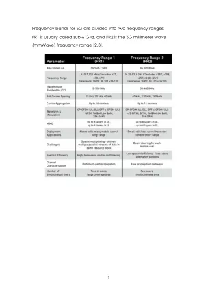
Frequency bands for 5G are divided into two frequency ranges: FR1 is usually called sub-6 GHz, and FR2 is the 5G millimeter wave (mmWave) frequency range [2,3]. 1
FR1 aims to integrate sub-6GHz bands initially to provide seamless transition from 4G to 5G. FR2, or mm-wave, can provide large bandwidth due to numerous unused bands, thereby augmenting data rate. 2
4G/5G RF front end diagram is as shown above [2]. It increases the number of antennas to 6-8 with the requirement to reach these antennas from different 4G/5G LTE radios which have to coexist with multiple WiFi & WiFi 6 radios, Bluetooth, GPS and UWB. The bands dedicated to FR1 are n77/n78 (3.3-4.2 GHz), n79 (4.4-4.5 GHz) and eLAA bands B46, B47 (5.15 GHz-5.92 GHz). Indeed, in FR1, wider bandwidth brings higher PAPR, so ET (Envelope Tracking) technique is still required. 3
Power Class 2 is a new LTE power standard to improve high-performance user equipment (HPUE) and TDD bands’ coverage worldwide [4]. Power Class 2 allows for output power levels of 26 dBm — double the maximum output power previously defined by Power Class 3 (23 dBm). It will allow 19% increase in cell coverage radius (42% increases in the base-station coverage area). The increase in output power compensates for more significant propagation losses at the higher TDD frequencies, enabling carriers to maintain cell coverage without adding expensive infrastructure. Indeed, this brings more challenging requirements on PA linearity and power consumption, which aggravates the thermal issue as well. 4
There are two basic deployment scenarios for 4G transition to 5G networks: 5G standalone (SA) deployment and non-standalone (NSA) deployment. For NSA deployment UE should support dual connectivity (DC) for 4G LTE and 5G NR. DC will combine the coverage advantage of existing 4G LTE networks with the higher DR throughput and latency advantages of 5G NR. When 4G FDD LTE and 5G NR are implemented, there are more challenges of intermodulation (IMD) distortions due to more than one Tx in UL together with several Rx in DL as well WiFi and other radios which will create RF interference through conductive and radiated paths. This brings a more strict linearity requirement on RF front-ends [2]. 5
There are a few types of interference due to simultaneous UL and DL over different bands in CA configurations which will degrade the Rx sensitivity (desense): 1.Harmonic products: For example, when a UE is transmitting on LTE Band 3 (1800 MHz) and receiving on 5G NR bands n77/n78 (3300 MHz ~ 4200 MHz), second harmonic of Band 3 will fall into 5G NR Rx for bands n77/n78. 2.Intermodulation (IMD) To avoid any desense due to third harmonic, at least 90 dB attenuation/isolation is required and very challenging even using FEMiD shielding. 6
One thing is worth mentioning; the B17 TX signal may couple to B4 RX path due to poor isolation between traces. Thus, lay either LB or MB traces in the inner layers for better isolation. Otherwise, both TX and harmonic distortion from B17 may couple to B4 RX path simultaneously. And, B17 TX may produce harmonic product through the nonlinearity of ASM. That is, the total harmonic product level would be the summation of the two interferences. If both of them are -90 dBm, then the whole harmonic product level would be -87 dBm [5]. 7
Additionally, the isolation between the primary antenna and the secondary antenna is crucial as well. The worst case is the B4 DRX signal would be interfered by B4 TX, B17 TX, and B17 3f0 simultaneously if the isolation is not large enough. 8
Thus, the locations of main and diversity antennas inside a cellphone are as shown above, the primary antenna is usually on the bottom side, and the diversity antenna is generally on the top side. In addition to enhancing the antenna-to-antenna isolation, we put the primary antenna on the bottom side to mitigate SAR (Specific Absorption Rate) issue. Besides, the linearity of the impedance tuner and aperture tuner should be high enough since they have to handle LB and HB TX signals simultaneously. Otherwise, the harmonic distortion and the intermodulation due to the nonlinearity of these two devices may result in interference issues as well. 9
For a 10 MHz wide signal, interference should be less than -115 dBm, and then the total noise floor (thermal noise + interference) rises 0.3 dB, and we can say the desense is 0.3 dB as well, which can be omitted. That is, for a 10 MHz LTE signal, the co-channel interference should be less than -115 dBm. To put it another way, if we assume the IMD distortion that falls into RX band -115 dBm, and the two TX tones 23 dBm. The IIP3 should be less than: And the answer is 92 dBm. Consequently, the IIP3 of tuning elements should be larger than 92 dBm. 10
It’s well known that Envelope Tracking (ET) is a power supply technique for improving the efficiency of PAs by tracking the envelope as opposed to today’s fixed power systems. Because intra-band CA involves the transmission of wideband signals with high peak-to-average ratios, which results in more power consumption. Consequently, for the CA case, ET is more crucial than the non-CA case [6]. 11
For ET, the Vcc and the RF input signal must be aligned in time of the PA. Otherwise, these will be a time delay between RF input signal and Vcc, thereby aggravating transmitter performance, such as ACLR and EVM [6]. 12
Thus, proper time delay adjustment is necessary. The intermodulation distortion introduced by the delay mismatch is given by: where BRF is the bandwidth of the RF signal and is the delay mismatch [2]. Since ACLR is just the intermodulation product, it indicates that ACLR performance is sensitive to delay mismatch for the wideband signal. 13
As shown above, with 1ns delay mismatch, the ACLR aggravates merely 1 dB for the 1.4 MHz signal, but 15 dB for the 60 MHz signal (3CA). 14
Reference [1] 5G RF For Dummies®, 2nd Qorvo Special Edition [2] RF Front End Module Architectures for 5G [3] Exploring 5G RF Technology [4] Power Class 2: What You Need to Know, Qorvo [5] ABCs of Carrier Aggregation [6] Enabling Carrier Aggregation 15